参数资料
| 型号: | XCV812E-8BG560C |
| 厂商: | Xilinx Inc |
| 文件页数: | 23/118页 |
| 文件大小: | 0K |
| 描述: | IC FPGA 1.8V C-TEMP 560-MBGA |
| 产品变化通告: | FPGA Family Discontinuation 18/Apr/2011 |
| 标准包装: | 1 |
| 系列: | Virtex®-E EM |
| LAB/CLB数: | 4704 |
| 逻辑元件/单元数: | 21168 |
| RAM 位总计: | 1146880 |
| 输入/输出数: | 404 |
| 门数: | 254016 |
| 电源电压: | 1.71 V ~ 1.89 V |
| 安装类型: | 表面贴装 |
| 工作温度: | 0°C ~ 85°C |
| 封装/外壳: | 560-LBGA,金属 |
| 供应商设备封装: | 560-MBGA(42.5x42.5) |
第1页第2页第3页第4页第5页第6页第7页第8页第9页第10页第11页第12页第13页第14页第15页第16页第17页第18页第19页第20页第21页第22页当前第23页第24页第25页第26页第27页第28页第29页第30页第31页第32页第33页第34页第35页第36页第37页第38页第39页第40页第41页第42页第43页第44页第45页第46页第47页第48页第49页第50页第51页第52页第53页第54页第55页第56页第57页第58页第59页第60页第61页第62页第63页第64页第65页第66页第67页第68页第69页第70页第71页第72页第73页第74页第75页第76页第77页第78页第79页第80页第81页第82页第83页第84页第85页第86页第87页第88页第89页第90页第91页第92页第93页第94页第95页第96页第97页第98页第99页第100页第101页第102页第103页第104页第105页第106页第107页第108页第109页第110页第111页第112页第113页第114页第115页第116页第117页第118页
Virtex-E 1.8 V Extended Memory Field Programmable Gate Arrays
Module 2 of 4
DS025-2 (v3.0) March 21, 2014
8
R
— OBSOLETE — OBSOLETE — OBSOLETE — OBSOLETE —
DLL provides four quadrature phases of the source clock,
and can double the clock or divide the clock by 1.5, 2, 2.5, 3,
4, 5, 8, or 16.
The DLL also operates as a clock mirror. By driving the output
from a DLL off-chip and then back on again, the DLL can be
used to de-skew a board level clock among multiple devices.
In order to guarantee that the system clock is operating cor-
rectly prior to the FPGA starting up after configuration, the
DLL can delay the completion of the configuration process
until after it has achieved lock.
For more information about DLL functionality, see the
Design Consideration section of the data sheet.
Boundary Scan
Virtex-E devices support all the mandatory boundary-scan
instructions specified in the IEEE standard 1149.1. A Test
Access Port (TAP) and registers are provided that imple-
ment the EXTEST, INTEST, SAMPLE/PRELOAD, BYPASS,
IDCODE, USERCODE, and HIGHZ instructions. The TAP
also supports two internal scan chains and configura-
tion/readback of the device.
The JTAG input pins (TDI, TMS, TCK) do not have a VCCO
requirement, and operate with either 2.5 V or 3.3 V input
signalling levels. The output pin (TDO) is sourced from the
VCCO in bank 2, and for proper operation of LVTTL 3.3 V
levels, the bank should be supplied with 3.3 V.
Boundary-scan operation is independent of individual IOB
configurations, and unaffected by package type. All IOBs,
including un-bonded ones, are treated as independent
3-state bidirectional pins in a single scan chain. Retention of
the bidirectional test capability after configuration facilitates
the testing of external interconnections, provided the user
design or application is turned off.
Table 6 lists the boundary-scan instructions supported in
Virtex-E FPGAs. Internal signals can be captured during
EXTEST by connecting them to un-bonded or unused IOBs.
They can also be connected to the unused outputs of IOBs
defined as unidirectional input pins.
Before the device is configured, all instructions except
USER1 and USER2 are available. After configuration, all
instructions are available. During configuration, it is recom-
mended that those operations using the boundary-scan
register (SAMPLE/PRELOAD, INTEST, EXTEST) not be
performed.
In addition to the test instructions outlined above, the
boundary-scan circuitry can be used to configure the
FPGA, and also to read back the configuration data.
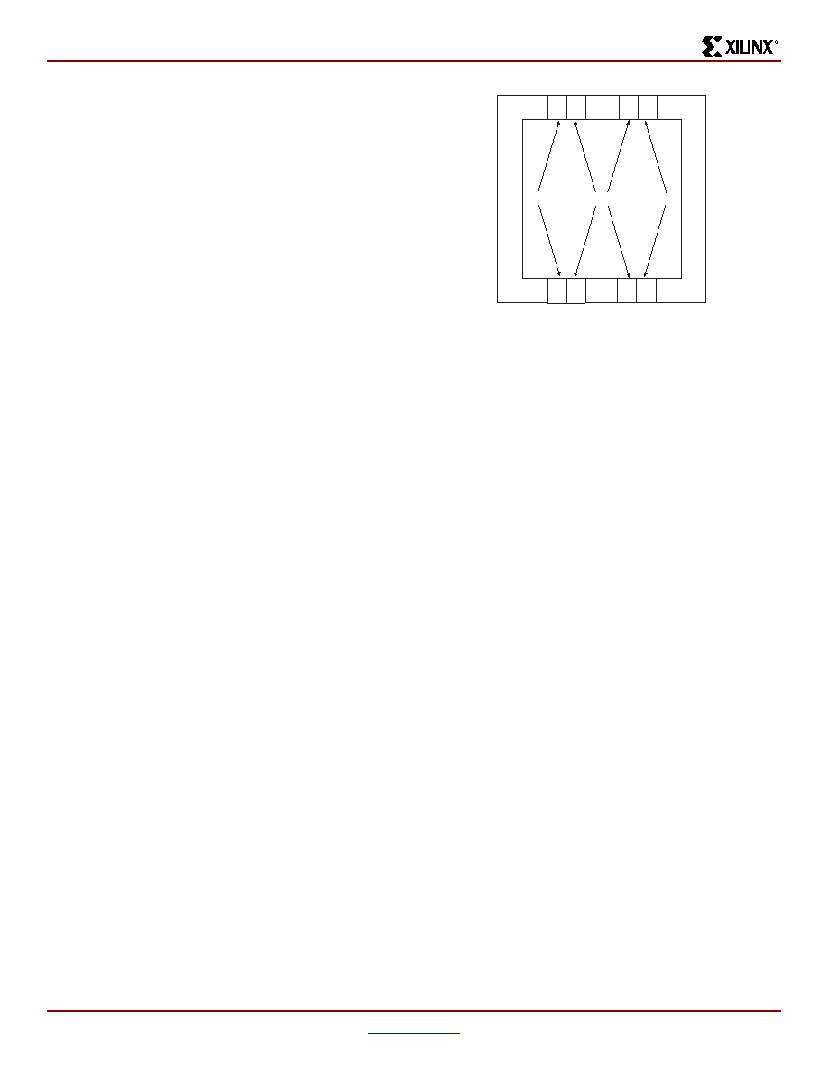
Figure 10: DLL Locations
XCVE_0010
DLLDLL
Primary DLLs
Secondar
y
DLLs
Secondar
y
DLLs
DLLDLL
相关PDF资料 |
PDF描述 |
|---|---|
| XC6VSX315T-L1FFG1156C | IC FPGA VIRTEX 6 314K 1156FFGBGA |
| AMM31DRMI | CONN EDGECARD 62POS .156 WW |
| XC6VSX315T-2FFG1156C | IC FPGA VIRTEX 6 314K 1156FFGBGA |
| XC6VLX365T-1FFG1759C | IC FPGA VIRTEX 6 364K 1759FFGBGA |
| XC6VLX240T-L1FF1759I | IC FPGA VIRTEX-6LXT 1759FFBGA |
相关代理商/技术参数 |
参数描述 |
|---|---|
| XCV812E-8BG560I | 制造商:XILINX 制造商全称:XILINX 功能描述:Virtex-E 1.8 V Extended Memory Field Programmable Gate Arrays |
| XCV812E-8BG676C | 制造商:XILINX 制造商全称:XILINX 功能描述:Virtex-E 1.8 V Extended Memory Field Programmable Gate Arrays |
| XCV812E-8BG676I | 制造商:XILINX 制造商全称:XILINX 功能描述:Virtex-E 1.8 V Extended Memory Field Programmable Gate Arrays |
| XCV812E-8BG900C | 制造商:XILINX 制造商全称:XILINX 功能描述:Virtex-E 1.8 V Extended Memory Field Programmable Gate Arrays |
| XCV812E-8BG900I | 制造商:XILINX 制造商全称:XILINX 功能描述:Virtex-E 1.8 V Extended Memory Field Programmable Gate Arrays |
发布紧急采购,3分钟左右您将得到回复。