参数资料
| 型号: | XCV812E-8BG560C |
| 厂商: | Xilinx Inc |
| 文件页数: | 85/118页 |
| 文件大小: | 0K |
| 描述: | IC FPGA 1.8V C-TEMP 560-MBGA |
| 产品变化通告: | FPGA Family Discontinuation 18/Apr/2011 |
| 标准包装: | 1 |
| 系列: | Virtex®-E EM |
| LAB/CLB数: | 4704 |
| 逻辑元件/单元数: | 21168 |
| RAM 位总计: | 1146880 |
| 输入/输出数: | 404 |
| 门数: | 254016 |
| 电源电压: | 1.71 V ~ 1.89 V |
| 安装类型: | 表面贴装 |
| 工作温度: | 0°C ~ 85°C |
| 封装/外壳: | 560-LBGA,金属 |
| 供应商设备封装: | 560-MBGA(42.5x42.5) |
第1页第2页第3页第4页第5页第6页第7页第8页第9页第10页第11页第12页第13页第14页第15页第16页第17页第18页第19页第20页第21页第22页第23页第24页第25页第26页第27页第28页第29页第30页第31页第32页第33页第34页第35页第36页第37页第38页第39页第40页第41页第42页第43页第44页第45页第46页第47页第48页第49页第50页第51页第52页第53页第54页第55页第56页第57页第58页第59页第60页第61页第62页第63页第64页第65页第66页第67页第68页第69页第70页第71页第72页第73页第74页第75页第76页第77页第78页第79页第80页第81页第82页第83页第84页当前第85页第86页第87页第88页第89页第90页第91页第92页第93页第94页第95页第96页第97页第98页第99页第100页第101页第102页第103页第104页第105页第106页第107页第108页第109页第110页第111页第112页第113页第114页第115页第116页第117页第118页
Virtex-E 1.8 V Extended Memory Field Programmable Gate Arrays
DS025-3 (v3.0) March 21, 2014
Module 3 of 4
13
R
— OBSOLETE — OBSOLETE — OBSOLETE — OBSOLETE —
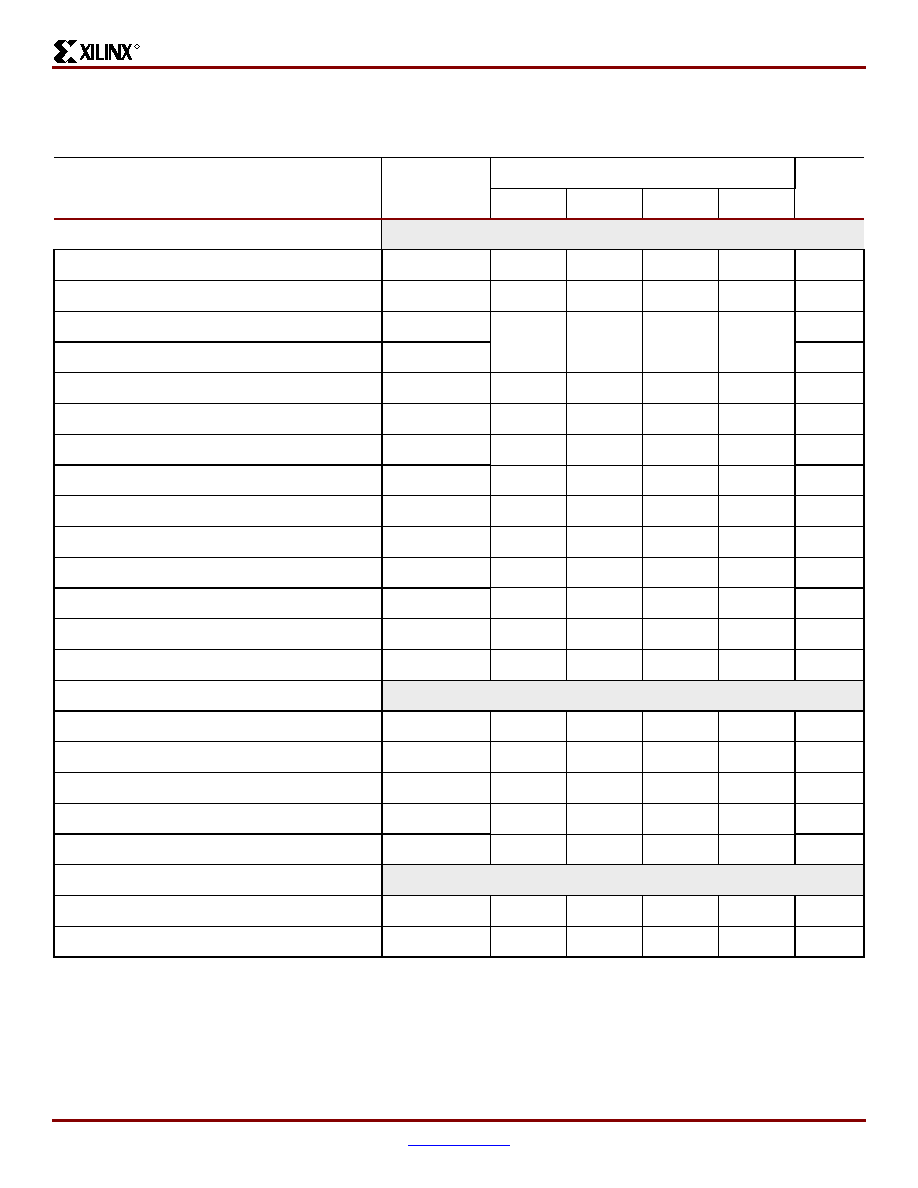
CLB Arithmetic Switching Characteristics
Setup times not listed explicitly can be approximated by decreasing the combinatorial delays by the setup time adjustment
listed. Precise values are provided by the timing analyzer.
Description(1)
Symbol
Speed Grade
Units
Min
-8
-7
-6
Combinatorial Delays
F operand inputs to X via XOR
TOPX
0.32
0.68
0.8
ns, max
F operand input to XB output
TOPXB
0.35
0.65
0.8
0.9
ns, max
F operand input to Y via XOR
TOPY
0.59
1.07
1.4
1.5
ns, max
F operand input to YB output
TOPYB
0.48
0.89
1.1
1.3
ns, max
F operand input to COUT output
TOPCYF
0.37
0.71
0.9
1.0
ns, max
G operand inputs to Y via XOR
TOPGY
0.34
0.72
0.8
0.9
ns, max
G operand input to YB output
TOPGYB
0.47
0.78
1.2
1.3
ns, max
G operand input to COUT output
TOPCYG
0.36
0.60
0.9
1.0
ns, max
BX initialization input to COUT
TBXCY
0.19
0.36
0.51
0.57
ns, max
CIN input to X output via XOR
TCINX
0.27
0.50
0.6
0.7
ns, max
CIN input to XB
TCINXB
0.02
0.04
0.07
0.08
ns, max
CIN input to Y via XOR
TCINY
0.26
0.45
0.7
ns, max
CIN input to YB
TCINYB
0.16
0.28
0.38
0.43
ns, max
CIN input to COUT output
TBYP
0.05
0.10
0.14
0.15
ns, max
Multiplier Operation
F1/2 operand inputs to XB output via AND
TFANDXB
0.10
0.30
0.35
0.39
ns, max
F1/2 operand inputs to YB output via AND
TFANDYB
0.28
0.56
0.7
0.8
ns, max
F1/2 operand inputs to COUT output via AND
TFANDCY
0.17
0.38
0.46
0.51
ns, max
G1/2 operand inputs to YB output via AND
TGANDYB
0.20
0.46
0.55
0.7
ns, max
G1/2 operand inputs to COUT output via AND
TGANDCY
0.09
0.28
0.30
0.34
ns, max
Setup and Hold Times before/after Clock CLK
CIN input to FFX
TCCKX/TCKCX
0.47 / 0
1.0 / 0
1.2 / 0
1.3 / 0
ns, min
CIN input to FFY
TCCKY/TCKCY
0.49 / 0
0.92 / 0
1.2 / 0
1.3 / 0
ns, min
Notes:
1.
A Zero “0” Hold Time listing indicates no hold time or a negative hold time. Negative values can not be guaranteed “best-case”, but
if a “0” is listed, there is no positive hold time.
相关PDF资料 |
PDF描述 |
|---|---|
| XC6VSX315T-L1FFG1156C | IC FPGA VIRTEX 6 314K 1156FFGBGA |
| AMM31DRMI | CONN EDGECARD 62POS .156 WW |
| XC6VSX315T-2FFG1156C | IC FPGA VIRTEX 6 314K 1156FFGBGA |
| XC6VLX365T-1FFG1759C | IC FPGA VIRTEX 6 364K 1759FFGBGA |
| XC6VLX240T-L1FF1759I | IC FPGA VIRTEX-6LXT 1759FFBGA |
相关代理商/技术参数 |
参数描述 |
|---|---|
| XCV812E-8BG560I | 制造商:XILINX 制造商全称:XILINX 功能描述:Virtex-E 1.8 V Extended Memory Field Programmable Gate Arrays |
| XCV812E-8BG676C | 制造商:XILINX 制造商全称:XILINX 功能描述:Virtex-E 1.8 V Extended Memory Field Programmable Gate Arrays |
| XCV812E-8BG676I | 制造商:XILINX 制造商全称:XILINX 功能描述:Virtex-E 1.8 V Extended Memory Field Programmable Gate Arrays |
| XCV812E-8BG900C | 制造商:XILINX 制造商全称:XILINX 功能描述:Virtex-E 1.8 V Extended Memory Field Programmable Gate Arrays |
| XCV812E-8BG900I | 制造商:XILINX 制造商全称:XILINX 功能描述:Virtex-E 1.8 V Extended Memory Field Programmable Gate Arrays |
发布紧急采购,3分钟左右您将得到回复。