参数资料
| 型号: | XRD9836ACG |
| 厂商: | Exar Corporation |
| 文件页数: | 6/32页 |
| 文件大小: | 0K |
| 描述: | IC 16B CCD/CIS SIG PROC 48TSSOP |
| 产品变化通告: | Leaded UART, V&I Obsolescence 11/Apr/2011 |
| 标准包装: | 39 |
| 位数: | 16 |
| 通道数: | 3 |
| 功率(瓦特): | 500mW |
| 电压 - 电源,模拟: | 3 V ~ 3.6 V |
| 电压 - 电源,数字: | 3 V ~ 3.6 V |
| 封装/外壳: | 48-TSSOP(0.240",6.10mm 宽) |
| 供应商设备封装: | 48-TSSOP |
| 包装: | 管件 |
第1页第2页第3页第4页第5页当前第6页第7页第8页第9页第10页第11页第12页第13页第14页第15页第16页第17页第18页第19页第20页第21页第22页第23页第24页第25页第26页第27页第28页第29页第30页第31页第32页
XRD9836
xr
16-BIT PIXEL GAIN AFE
REV. 1.0.0
14
TIMING - CLOCK BASICS:
The XRD9836 has 4 clock signals BSAMP, VSAMP,
ADCLK and LCLMP. These inputs control the sam-
pling, clamping and synchronization functions of the
device.
The pixel rate clocks are BSAMP, VSAMP and AD-
CLK. BSAMP controls the sampling of the black refer-
ence level of a CCD input signal. VSAMP controls the
sampling of the video level of a CCD or CIS output
signal. The ADCLK controls the internal sampling of
the PGA by the ADC and ADC operation.
The line rate clock, LCLMP, performs the clamping
and synchronization functions. The clamp function
sets the bias point for the external AC coupling ca-
pacitor on the inputs. Synchronization defines the odd
pixel in the APOAM mode.
CLOCK POLARITY
Each of the 4 timing signals has a separate polarity
control bit in the CONTROL register. Figure 10 shows
the logic implementation of the polarity control. If the
polarity bit is low (default) BSAMP and VSAMP sam-
ple on the falling edge, LCLMP is active high and AD-
CLK must be low during the VSAMP falling edge. See
timing examples if Figure 17 and Figure 18
If any of the external timing signals are inverted from
the default timing simply write a “1” to the appropriate
polarity bit to compensate.
DELAY CONTROL
One of the more difficult tasks in designing a scanner
is optimizing the pixel and interface (data output &
OGI) timing for a CCD, CDS and ADC. The
XRD9836 has included a programmable delay func-
tion to help simplify this job.
There are four serial interface registers, DelayA, De-
layB, DelayC and DelayD, used to program various
delays of the pixel timing and Data and OGI bus tim-
ing. Each register is divided into 2 delay parameters.
Each delay parameter is 4 bits wide.
DelayA[7:4] controls the OGI sampling delay. These
bits program the delay of the ADCLK used to sample
the OGI input bus. Delay is added in 1ns increments.
See Figure 12.
DelayA[3:0] controls the ADCDO delay. These bits
are used to program the timing delay added to the
ADCDO data bus updates. Delay is added in 1ns in-
crements. See Figure 11.
DelayB[7:4] controls the amount of delay added to the
leading edge of BSAMP. Delay to the leading edge
will be added in 0.5ns increments. This can help to
position the leading edge of the internal BSAMP away
from the reset pulse of the CCD input. See Figure 11.
DelayB[3:0] controls the amount of delay added to the
trailing edge of BSAMP. Delay to the trailing edge will
be added in 0.5ns increments. This will allow for ad-
justment of the Black Level sampling position by the
internal BSAMP. See Figure 11.
DelayC[7:4] controls the amount of delay added to
the leading edge of VSAMP. Delay will be added in
0.5ns increments. This can help to position the lead-
ing edge of the internal VSAMP to track the video
portion of the CCD input. See Figure 11.
DelayC[3:0] controls the amount of delay added to
the trailing edge of VSAMP. Delay will be added in
0.5ns increments. This will allow for adjustment of the
Video Level sampling position by the internal VSAMP.
See Figure 11.
DelayD[7:4] controls the amount of delay added to
the VSAMP OGI. The internal VSAMP_OGI is used
to transfer the input OGI register data to the PGA and
OFFSET control. Delay is added in 1ns increments.
Please note the falling edge of the internal
VSAMP_OGI must occur before the rising edge of
the OGI sampling clock. See Figure 12.
DelayD[3:0] controls the amount of delay added to
the ADCLK. Delay is added to the internal ADCLK in
0.5ns increments. See Figure 11.
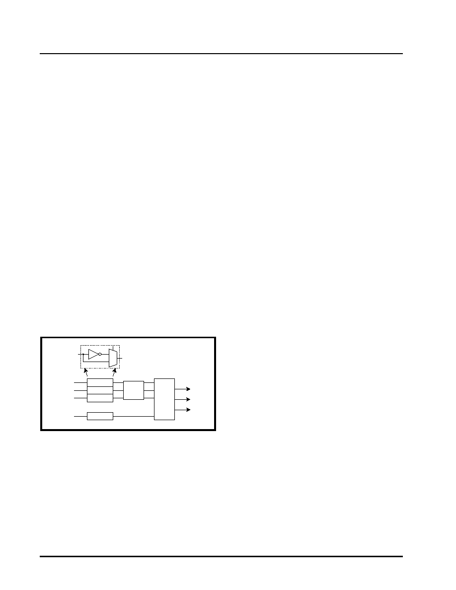
FIGURE 10. CLOCK POLARITY AND DELAYS
Polarity
Delays
Clock
Logic
BSAMP
VSAMP
ADCLK
LCLMP
Polarity
AFE
ADC
OGI
相关PDF资料 |
PDF描述 |
|---|---|
| XRD98L23ACU | IC 8B CCD/CIS SIG PROC 20SSOP |
| XRD98L59AIGTR | IC CCD DIGITIZER 10BIT 28TSSOP |
| XRD98L61AIV-F | IC CCD DIGITIZER 12BIT 48TQFP |
| XRD98L62ACV-F | IC CCD DIGITIZER 12BIT 48TQFP |
| XRD98L63AIV-F | IC CCD DIGITIZER 12BIT 48TQFP |
相关代理商/技术参数 |
参数描述 |
|---|---|
| XRD9836ACG-F | 功能描述:电信线路管理 IC RoHS:否 制造商:STMicroelectronics 产品:PHY 接口类型:UART 电源电压-最大:18 V 电源电压-最小:8 V 电源电流:30 mA 最大工作温度:+ 85 C 最小工作温度:- 40 C 安装风格:SMD/SMT 封装 / 箱体:VFQFPN-48 封装:Tray |
| XRD9836ACGTR-F | 功能描述:模数转换器 - ADC RoHS:否 制造商:Texas Instruments 通道数量:2 结构:Sigma-Delta 转换速率:125 SPs to 8 KSPs 分辨率:24 bit 输入类型:Differential 信噪比:107 dB 接口类型:SPI 工作电源电压:1.7 V to 3.6 V, 2.7 V to 5.25 V 最大工作温度:+ 85 C 安装风格:SMD/SMT 封装 / 箱体:VQFN-32 |
| XRD9853AIV | 制造商:EXAR 制造商全称:EXAR 功能描述:CCD Image Digitizers with CDS, PGA, and 10-bit A/D |
| XRD9855 | 制造商:EXAR 制造商全称:EXAR 功能描述:CCD Image Digitizers with CDS, PGA and 10-Bit A/D |
| XRD9855AIV | 制造商:EXAR 制造商全称:EXAR 功能描述:CCD Image Digitizers with CDS, PGA and 10-Bit A/D |
发布紧急采购,3分钟左右您将得到回复。