参数资料
| 型号: | XRD98L62ACV-F |
| 厂商: | Exar Corporation |
| 文件页数: | 24/37页 |
| 文件大小: | 0K |
| 描述: | IC CCD DIGITIZER 12BIT 48TQFP |
| 标准包装: | 250 |
| 位数: | 12 |
| 通道数: | 1 |
| 电压 - 电源,模拟: | 2.7 V ~ 3.6 V |
| 电压 - 电源,数字: | 2.7 V ~ 3.6 V |
| 封装/外壳: | 48-TQFP |
| 供应商设备封装: | 48-TQFP(7x7) |
| 包装: | 托盘 |
第1页第2页第3页第4页第5页第6页第7页第8页第9页第10页第11页第12页第13页第14页第15页第16页第17页第18页第19页第20页第21页第22页第23页当前第24页第25页第26页第27页第28页第29页第30页第31页第32页第33页第34页第35页第36页第37页
XRD98L62
30
Rev. P2.00
Preliminary
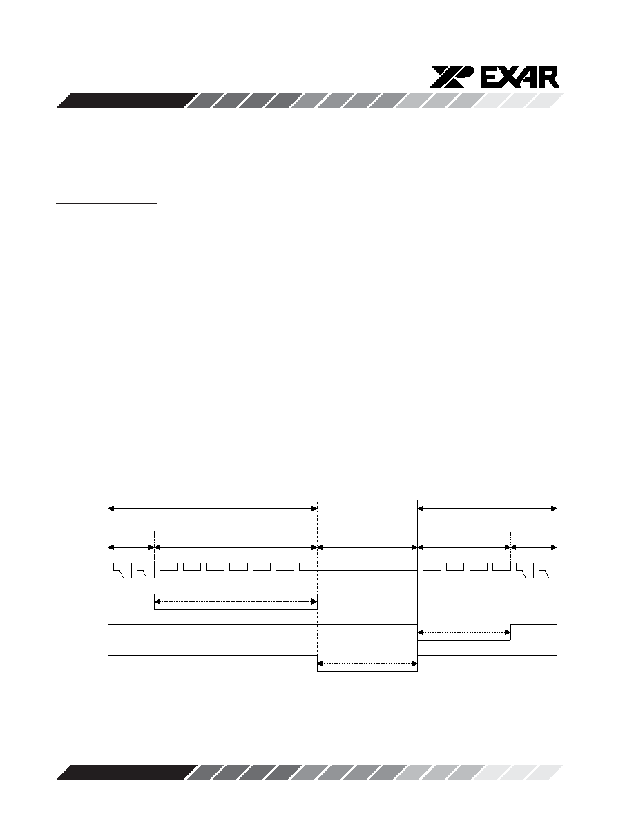
Line Rate Clocks
CLAMP & CAL are the two line rate clock signals.
There are two modes of operation for these clocks.
CAL & CLAMP Mode
In this mode the CLAMP signal is used to activate the
DC restore Clamp at the CDS input, and the CAL signal
is used to define the Optical Black pixels to be used for
the Black Level calibration function. Typically the
CLAMP pulse comes during the dummy or optical
black pixels at the beginning of each scan line, and the
CAL pulse comes during the longer string of optical
black pixels at the end of each scan line. CLAMP &
CAL must not be active at the same time.
In this mode there is an option to disconnect the CDS
from the input pins during the Vertical Shift time. To
enable this option write a “1” to the VSreject bit in the
Clock register. To properly define the Vertical Shift time
you must set the ClampCal bit properly.
In the typical case, the CCD has a few OB pixels at the
beginning of a line (CLAMP time) and a larger number
of OB pixels at the end of a scan line (CAL time). In this
case set the ClampCal bit = 0, this will define the
Vertical shift time as the time from the end of the CAL
pulse to the beginning of the CLAMP pulse.
If a CCD has more OB pixels at the beginning of a line,
then CAL should be active during these pixels and
CLAMP should be active at the end of the line. In this
case, set the ClampCal bit = 1, this will define the
Vertical shift time as the time from the end of the
CLAMP pulse to the beginning of the CAL pulse.
The ClampCal bit is also used by the Calibration logic.
If ClampCal is set as defined above, it should be correct
for the Calibration logic as well.
End of Line N
Start of Line N+1
Active Video
Pixels
OB pixels
Vertical Shift
Dummy &
OB pixels
CAL
(Black Level)
CLAMP
(DC restore)
CCD
Signal
Active Video pixels
t
CAL
t
CLAMP
Vert. Shift Reject
(internal)
Disconnect CDS from
input pins
Figure 20. Line Rate Timing with OneShot=0, VSreject=1 & ClampCal=0
相关PDF资料 |
PDF描述 |
|---|---|
| XRD98L63AIV-F | IC CCD DIGITIZER 12BIT 48TQFP |
| XRT71D00IQ-F | IC JITTER ATTENUATOR SGL 32TQFP |
| XRT71D03IV-F | IC JITTER ATTENUATOR 3CH 64TQFP |
| XRT71D04IV | IC JITTER ATTENUATOR 4CH 80TQFP |
| XRT8000IP-F | IC WAN CLOCK E1/E1 DUAL 18PDIP |
相关代理商/技术参数 |
参数描述 |
|---|---|
| XRD98L62EVAL | 功能描述:数据转换 IC 开发工具 XRD98L62 EVAL BOARD RoHS:否 制造商:Texas Instruments 产品:Demonstration Kits 类型:ADC 工具用于评估:ADS130E08 接口类型:SPI 工作电源电压:- 6 V to + 6 V |
| XRD98L62ZEVAL | 功能描述:数据转换 IC 开发工具 Eval Board (Solder) XRD98L62AIV RoHS:否 制造商:Texas Instruments 产品:Demonstration Kits 类型:ADC 工具用于评估:ADS130E08 接口类型:SPI 工作电源电压:- 6 V to + 6 V |
| XRD98L63 | 制造商:EXAR 制造商全称:EXAR 功能描述:CCD Image Digitizers with CDS, PGA and 12-Bit A/D |
| XRD98L63AIV | 制造商:EXAR 制造商全称:EXAR 功能描述:CCD Image Digitizers with CDS, PGA and 12-Bit A/D |
| XRD98L63AIV-F | 功能描述:模数转换器 - ADC RoHS:否 制造商:Texas Instruments 通道数量:2 结构:Sigma-Delta 转换速率:125 SPs to 8 KSPs 分辨率:24 bit 输入类型:Differential 信噪比:107 dB 接口类型:SPI 工作电源电压:1.7 V to 3.6 V, 2.7 V to 5.25 V 最大工作温度:+ 85 C 安装风格:SMD/SMT 封装 / 箱体:VQFN-32 |
发布紧急采购,3分钟左右您将得到回复。