参数资料
| 型号: | XRT75L06DIB-F |
| 厂商: | Exar Corporation |
| 文件页数: | 39/103页 |
| 文件大小: | 0K |
| 描述: | IC LIU E3/DS3/STS-1 6CH 217BGA |
| 标准包装: | 60 |
| 类型: | 线路接口装置(LIU) |
| 驱动器/接收器数: | 6/6 |
| 规程: | DS3,E3,STS-1 |
| 电源电压: | 3.135 V ~ 3.465 V |
| 安装类型: | 表面贴装 |
| 封装/外壳: | 217-BBGA |
| 供应商设备封装: | 217-BGA(23x23) |
| 包装: | 托盘 |
第1页第2页第3页第4页第5页第6页第7页第8页第9页第10页第11页第12页第13页第14页第15页第16页第17页第18页第19页第20页第21页第22页第23页第24页第25页第26页第27页第28页第29页第30页第31页第32页第33页第34页第35页第36页第37页第38页当前第39页第40页第41页第42页第43页第44页第45页第46页第47页第48页第49页第50页第51页第52页第53页第54页第55页第56页第57页第58页第59页第60页第61页第62页第63页第64页第65页第66页第67页第68页第69页第70页第71页第72页第73页第74页第75页第76页第77页第78页第79页第80页第81页第82页第83页第84页第85页第86页第87页第88页第89页第90页第91页第92页第93页第94页第95页第96页第97页第98页第99页第100页第101页第102页第103页
XRT75L06D
xr
SIX CHANNEL E3/DS3/STS-1 LINE INTERFACE UNIT WITH SONET DESYNCHRONIZER
REV. 1.0.4
36
4.2
JITTER TRANSFER
Jitter Transfer function is defined as the ratio of jitter on the output relative to the jitter applied on the input
versus frequency. There are two distinct characteristics in jitter transfer, jitter gain (jitter peaking) defined as
the highest ratio above 0dB and jitter transfer bandwidth. The overall jitter transfer bandwidth is controlled by a
low bandwidth loop, typically using a voltage-controlled crystal oscillator (VCXO).
The jitter transfer function is a ratio between the jitter output and jitter input for a component, or system often
expressed in dB. A negative dB jitter transfer indicates the element removed jitter. A positive dB jitter transfer
indicates the element added jitter. A zero dB jitter transfer indicates the element had no effect on jitter. Table 9
shows the jitter transfer characteristics and/or jitter attenuation specifications for various data rates:
NOTE: The above specifications can be met only with a jitter attenuator that supports E3/DS3/STS-1 rates.
4.3
Jitter Attenuator
An advanced crystal-less jitter attenuator per channel is included in the XRT75L06D. The jitter attenuator
requires no external crystal nor high-frequency reference clock. By clearing or setting the JATx/Rx_n bits in
the channel control registers selects the jitter attenuator either in the Receive or Transmit path on per channel
basis. The FIFO size can be either 16-bit or 32-bit. The bits JA0_n and JA1_n can be set to appropriate
combination to select the different FIFO sizes or to disable the Jitter Attenuator on a per channel basis. Data is
clocked into the FIFO with the associated clock signal (TxClk or RxClk) and clocked out of the FIFO with the
dejittered clock. When the FIFO is within two bits of overflowing or underflowing, the FIFO limit status bit, FL_n
is set to “1” in the Alarm status register. Reading this bit clears the FIFO and resets the bit into default state.
NOTE: It is recommended to select the 16-bit FIFO for delay-sensitive applications as well as for removing smaller amounts
of jitter. Table 10 specifies the jitter transfer mask requirements for various data rates:
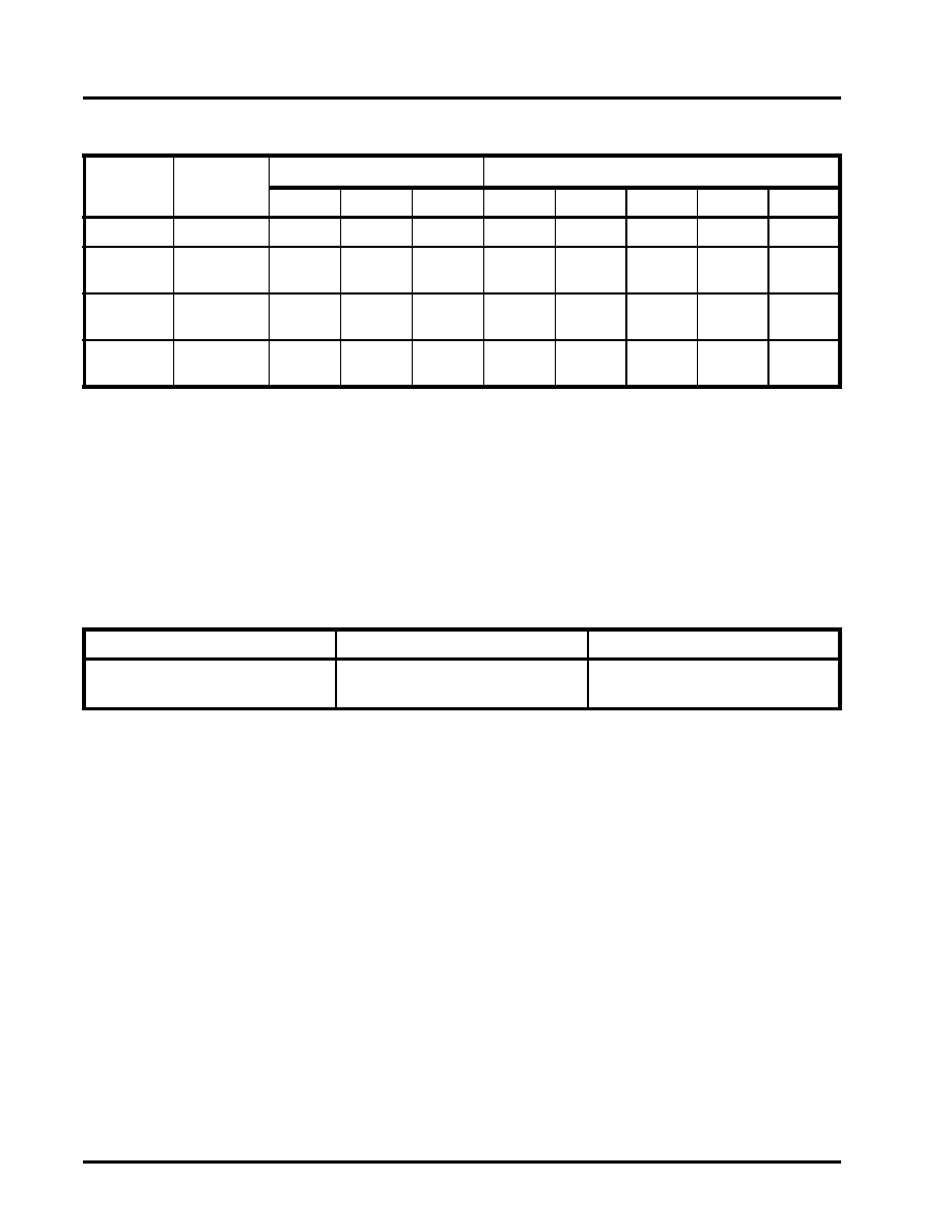
TABLE 8: JITTER AMPLITUDE VERSUS MODULATION FREQUENCY (JITTER TOLERANCE)
BIT RATE
(KB/S)
STANDARD
INPUT JITTER AMPLITUDE (UI
P
-P)
MODULATION FREQUENCY
A1
A2
A3
F
1(HZ)
F
2(HZ)
F
3(KHZ)
F
4(KHZ)
F
5(KHZ)
34368
ITU-T G.823
1.5
0.15
-
100
1000
10
800
-
44736
GR-499
CORE Cat I
5
0.1
-
10
2.3k
60
300
-
44736
GR-499
CORE Cat II
10
0.3
-
10
669
22.3
300
-
51840
GR-253
CORE Cat II
15
1.5
0.15
10
30
300
2
20
TABLE 9: JITTER TRANSFER SPECIFICATION/REFERENCES
E3
DS3
STS-1
ETSI TBR-24
GR-499 CORE section 7.3.2
Category I and Category II
GR-253 CORE section 5.6.2.1
相关PDF资料 |
PDF描述 |
|---|---|
| XRT75L06IB-F | IC LIU E3/DS3/STS-1 6CH 217BGA |
| XRT75R03DIV-F | IC LIU E3/DS3/STS-1 3CH 128LQFP |
| XRT75R03IV-F | IC LIU E3/DS3/STS-1 3CH 128LQFP |
| XRT75R06DIB-F | IC LIU E3/DS3/STS-1 6CH 217BGA |
| XRT75R06IB-F | IC LIU E3/DS3/STS-1 6CH 217BGA |
相关代理商/技术参数 |
参数描述 |
|---|---|
| XRT75L06ES | 功能描述:时钟合成器/抖动清除器 6 CHT3/E3/STS1 LIU+JA 3.3V RoHS:否 制造商:Skyworks Solutions, Inc. 输出端数量: 输出电平: 最大输出频率: 输入电平: 最大输入频率:6.1 GHz 电源电压-最大:3.3 V 电源电压-最小:2.7 V 封装 / 箱体:TSSOP-28 封装:Reel |
| XRT75L06IB | 功能描述:接口 - 专用 6CH E3/DS3/STS1 LIU+Jitter Attenuato RoHS:否 制造商:Texas Instruments 产品类型:1080p60 Image Sensor Receiver 工作电源电压:1.8 V 电源电流:89 mA 最大功率耗散: 最大工作温度:+ 85 C 安装风格:SMD/SMT 封装 / 箱体:BGA-59 |
| XRT75L06IB-F | 功能描述:外围驱动器与原件 - PCI 6-Ch DS3, E3, STS-1 RoHS:否 制造商:PLX Technology 工作电源电压: 最大工作温度: 安装风格:SMD/SMT 封装 / 箱体:FCBGA-1156 封装:Tray |
| XRT75R03 | 制造商:EXAR 制造商全称:EXAR 功能描述:THREE CHANNEL E3/DS3/STS-1 LINE INTERFACE UNIT WITH JITTER ATTENUATOR |
| XRT75R03D | 制造商:EXAR 制造商全称:EXAR 功能描述:THREE CHANNEL E3/DS3/STS-1 LINE INTERFACE UNIT WITH SONET DESYNCRONIZER |
发布紧急采购,3分钟左右您将得到回复。