- 您现在的位置:买卖IC网 > PDF目录19434 > ZL9101MIRZ (Intersil)MODULE DGTL DC-DC 12A 21QFN PDF资料下载
参数资料
| 型号: | ZL9101MIRZ |
| 厂商: | Intersil |
| 文件页数: | 5/19页 |
| 文件大小: | 0K |
| 描述: | MODULE DGTL DC-DC 12A 21QFN |
| 产品培训模块: | Solutions for Industrial Control Applications |
| 特色产品: | ZL9101M Digital DC/DC Power Module |
| 标准包装: | 96 |
| 系列: | ZL9101M |
| 类型: | 非隔离(POL) |
| 输出数: | 1 |
| 电压 - 输入(最小): | 4.5V |
| 电压 - 输入(最大): | 13.2V |
| Voltage - Output 1: | 0.6 ~ 4 V |
| 电流 - 输出(最大): | 12A |
| 电源(瓦) - 制造商系列: | 48W |
| 安装类型: | 表面贴装 |
| 封装/外壳: | 21-QFN,变式 |
| 尺寸/尺寸: | 0.59" L x 0.59" W x 0.14" H(15.0mm x 15.0mm x 3.5mm) |
| 包装: | 托盘 |
| 工作温度: | -40°C ~ 85°C |
| 效率: | 95% |
| 电源(瓦特)- 最大: | 48W |
�� �
�
�ZL9101M�
�Absolute� Maximum� Ratings� (Note� 4)�
�DC� Supply� Voltage� for� VDD� Pin� .� .� .� .� .� .� .� .� .� .� .� .� .� .� .� .� .� .� .� .� .� .� .� .� -0.3V� to� 15.7V�
�Input� Voltage� for� VIN� Pin� .� .� .� .� .� .� .� .� .� .� .� .� .� .� .� .� .� .� .� .� .� .� .� .� .� .� .� .� .� -0.3V� to� 15.7V�
�MOSFET� Drive� Reference� for� VR� Pin� .� .� .� .� .� .� .� .� .� .� .� .� .� .� .� .� .� .� .� .� -0.3V� to� 6.5V�
�2.5V� Logic� Reference� for� V25� Pin.� .� .� .� .� .� .� .� .� .� .� .� .� .� .� .� .� .� .� .� .� .� .� .� .� -0.3V� to� 3V�
�MOSFET� Driver� Power� for� VDRV� Pin� .� .� .� .� .� .� .� .� .� .� .� .� .� .� .� .� .� .� .� .� .� .-0.3V� to� 7.5V�
�Logic� I/O� Voltage� for� DDC,� EN,�
�FB+,� FB-,� PG,� SA,� SCL,� SDA,SYNC,� VSET� Pins� .� .� .� .� .� .� .� .� .� .� .� .� .� .� .� -0.3V� to� 6V�
�ESD� Rating�
�Human� Body� Model� (Tested� per� JESD22-A114F)� .� .� .� .� .� .� .� .� .� .� .� .� .� .� 2000V�
�Machine� Model� (Tested� per� JESD22-A115C)� .� .� .� .� .� .� .� .� .� .� .� .� .� .� .� .� .� .� 200V�
�Charged� Device� Model� (Tested� per� JESD22-C110D)� .� .� .� .� .� .� .� .� .� .� .� 1000V�
�Latch� Up� (Tested� per� JESD78C;� Class� 2,� Level� A)� .� .� .� .� .� .� .� .� .� .� .� .� .� .� .� 100mA�
�Thermal� Information�
�Thermal� Resistance� (Typical)� θ� JA� (°C/W)� θ� JC� (°C/W)�
�QFN� Package� (Notes� 7,� 8)� .� .� .� .� .� .� .� .� .� .� .� .� .� .� 11.5� 2.2�
�Junction� Temperature� .� .� .� .� .� .� .� .� .� .� .� .� .� .� .� .� .� .� .� .� .� .� .� .� .� .� .� .� .-55°C� to� +150°C�
�Storage� Temperature� .� .� .� .� .� .� .� .� .� .� .� .� .� .� .� .� .� .� .� .� .� .� .� .� .� .� .� .� .� .-55°C� to� +150°C�
�Pb-Free� Reflow� Profile� .� .� .� .� .� .� .� .� .� .� .� .� .� .� .� .� .� .� .� .� .� .� .� .� .� .� .� .� .� .� .� see� link� below�
�http://www.intersil.com/pbfree/Pb-FreeReflow.asp�
�Recommended� Operating� Conditions�
�Input� Supply� Voltage� Range,� V� IN� .� .� .� .� .� .� .� .� .� .� .� .� .� .� .� .� .� .� .� .� .� .� .� 4.5V� to� 13.2V�
�Input� Supply� For� Controller,� V� DD� (Note� 5)� .� .� .� .� .� .� .� .� .� .� .� .� .� .� .� .� 4.5V� to� 13.2V�
�Driver� Supply� Voltage,� V� DRV� .� .� .� .� .� .� .� .� .� .� .� .� .� .� .� .� .� .� .� .� .� .� .� .� .� .� .� .� 4.5V� to� 6.5V�
�Output� Voltage� Range,� V� OUT� (Note� 6).� .� .� .� .� .� .� .� .� .� .� .� .� .� .� .� .� .� .� .� 0.54V� to� 3.6V�
�Output� Current� Range,� I� OUT(DC)� .� .� .� .� .� .� .� .� .� .� .� .� .� .� .� .� .� .� .� .� .� .� .� .� .� .� .� 0A� to� 12A�
�Operating� Junction� Temperature� Range,� T� J� .� .� .� .� .� .� .� .� .� .� .� .� .� .� .� .� .� .� .� -40°C� to� +125°C�
�CAUTION:� Do� not� operate� at� or� near� the� maximum� ratings� listed� for� extended� periods� of� time.� Exposure� to� such� conditions� may� adversely� impact� product�
�reliability� and� result� in� failures� not� covered� by� warranty.�
�NOTES:�
�4.� Voltage� measured� with� respect� to� SGND�
�5.� V� IN� supplies� the� power� FETs.� V� DD� supplies� the� controller.� V� IN� can� be� tied� to� V� DD� .� For� V� DD� ≤� 5.5V,� V� DD� should� be� tied� to� VR.�
�6.� Includes� ±10%� margin� limits.�
�7.� θ� JA� is� simulated� in� free� air� with� device� mounted� on� a� four-layer� FR-4� test� board� (76.2� x� 114.3� x� 1.6mm)� with� 80%-coverage,� 2-ounce� Cu� on� top� and�
�bottom� layers,� plus� two,� buried,� one-ounce� Cu� layers� with� coverage� across� the� entire� test� board� area.� Multiple� vias� were� used,� with� via�
�diameter� =� 0.3mm� on� 1.2mm� pitch.�
�8.� For� θ� JC� ,� the� “case”� temperature� is� measured� at� the� center� of� the� package� underside.�
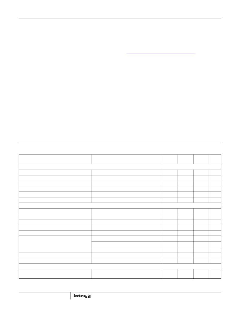
�Electrical� Specifications� V� DD� =� 12� V,� T� A� =� -40°C� to� +85°C� unless� otherwise� noted.� Typical� values� are� at� T� A� =� 25°C.� Boldface� limits� apply�
�over� the� operating� temperature� range,� -40°C� to� +85°C.�
�MIN�
�TYP�
�MAX�
�PARAMETER�
�CONDITIONS�
�(Note� 9)�
�(Note� 10)�
�(Note� 9)�
�UNIT�
�INPUT� AND� SUPPLY� CHARACTERISTICS�
�Input� Bias� Supply� Current,� I� DD�
�Input� Bias� Shutdown� Current,� I� DDS�
�Input� Supply� Current,� I� VIN�
�Driver� Supply� Current,� I� VDRV�
�VR� Reference� Output� Voltage� (Note� 11)�
�V25� Reference� Output� Voltage� (Note� 11)�
�f� SW� =� 571kHz,� No� load�
�EN� =� 0� V;� no� I� 2� C/SMBus� activity�
�V� IN� =� 13.2V,� I� OUT� =� 12A,� V� OUT� =� 1.2V�
�Not� switching�
�V� DD� >� 6V,� I� VR� <� 20mA�
�V� R� >� 3V,� I� V25� <� 20mA�
�–�
�–�
�–�
�–�
�4.5�
�2.25�
�20�
�15.5�
�1.32�
�190�
�5.2�
�2.5�
�40�
�20�
�–�
�250�
�5.7�
�2.75�
�mA�
�mA�
�A�
�μA�
�V�
�V�
�OUTPUT� CHARACTERISTICS�
�Output� Load� Current�
�V� IN� =� 12V,� V� OUT� =� 1.2V�
�12�
�A�
�Line� Regulation� Accuracy,� Δ� V� OUT� /� Δ� V� IN� (Note� 12)�
�Load� Regulation� Accuracy,� Δ� V� OUT� /� Δ� I� OUT� (Note� 12)�
�V� OUT� =� 1.2V,� I� OUT� =� 0A,� V� IN� =� 5V� to� 13.2V�
�I� OUT� =� 0A� to� 12A,� V� OUT� =� 1.2V�
�–�
�–�
�0.5�
�0.5�
�–�
�–�
�%�
�%�
�Peak-to-peak� Output� Ripple� Voltage,� Δ� V� OUT� (Note� 12)� I� OUT� =� 12A,� V� OUT� =� 1.2V,� C� OUT� =� 3000μF�
�–�
�6�
�–�
�mV�
�Soft-start� Delay� Duration� Range� (Notes� 11,� 13)�
�Soft-start� Delay� Duration� Accuracy� (Note� 11)�
�Soft-start� Ramp� Duration� Range� (Note� 11)�
�Soft-start� Ramp� Duration� Accuracy� (Note� 11)�
�Set� using� I� 2� C/SMBus�
�Turn-on� delay� (precise� mode)� (Notes� 13,� 14)�
�Turn-on� delay� (normal� mode)� (Note� 15)�
�Turn-off� delay� (Note� 15)�
�Set� using� I� 2� C�
�2�
�–�
�–�
�–�
�0�
�–�
�–�
�±0.25�
�-0.25/+4�
�-0.25/+4�
�–�
�100�
�200�
�-�
�-�
�-�
�200�
�–�
�ms�
�ms�
�ms�
�ms�
�ms�
�μs�
�DYNAMIC� CHARACTERISTICS�
�Voltage� Change� for� Positive� Load� Step�
�Δ� I� OUT� =� 6A,� slew� rate� =� 2.5A/� μ� s,�
�V� OUT� =� 1.2V,� C� OUT� =� 3000μF�
�–�
�3�
�–�
�%�
�5�
�FN7669.4�
�January� 20,� 2012�
�相关PDF资料 |
PDF描述 |
|---|---|
| EBM18DRKN-S13 | CONN EDGECARD 36POS .156 EXTEND |
| VI-B1F-CY-F1 | CONVERTER MOD DC/DC 72V 50W |
| VI-J32-IZ | CONVERTER MOD DC/DC 15V 25W |
| HWS30-12/A | PWR SUP IND 12V 2.5A SNG OUTPUT |
| 2211-H-RC | INDUCTOR TORD HI AMP 68UH HORZ |
相关代理商/技术参数 |
参数描述 |
|---|---|
| ZL9101MIRZ-T | 功能描述:DCDC DGTL PMBUS MODULE 12A 21QFN RoHS:是 类别:电源 - 板载 >> DC DC Converters 系列:ZL9101M 标准包装:10 系列:PT4570 类型:隔离 输出数:1 电压 - 输入(最小):36V 电压 - 输入(最大):75V Voltage - Output 1:9V Voltage - Output 2:- Voltage - Output 3:- 电流 - 输出(最大):3.3A 电源(瓦) - 制造商系列:30W 电压 - 隔离:1.5kV(1500V) 特点:- 安装类型:表面贴装 封装/外壳:19-SIP SMD 模块 尺寸/尺寸:3.00" L x 1.19" W x 0.50" H(76.2mm x 30.2mm x 12.7mm) 包装:托盘 工作温度:-40°C ~ 85°C 效率:84% 电源(瓦特)- 最大:30W |
| ZL9106MIRZ | 制造商:Intersil Corporation 功能描述:- Bulk |
| ZL9110MIRZ | 制造商:Intersil Corporation 功能描述:- Bulk |
| ZL9117EVAL1Z | 制造商:Intersil Corporation 功能描述:ZL9117EVAL1Z EVALUATION BOARD 1 - 21LD QFN -ROHS COMPLIAN - Bulk 制造商:Intersil Corporation 功能描述:BOARD EVAL FOR ZL9117M 制造商:Intersil Corporation 功能描述:ZL9117EVAL1Z EVALUATION BOARD 1 - 21LD QFN -RoHS COMPLIAN |
| ZL9117M | 制造商:INTERSIL 制造商全称:Intersil Corporation 功能描述:Digital DC/DC PMBus 17A Module |
发布紧急采购,3分钟左右您将得到回复。