- 您现在的位置:买卖IC网 > Datasheet目录538 > ZVN4310GTC (Diodes Inc)MOSFET N-CHAN 100V SOT223 Datasheet资料下载
参数资料
| 型号: | ZVN4310GTC |
| 厂商: | Diodes Inc |
| 文件页数: | 2/5页 |
| 文件大小: | 0K |
| 描述: | MOSFET N-CHAN 100V SOT223 |
| 标准包装: | 4,000 |
| FET 型: | MOSFET N 通道,金属氧化物 |
| FET 特点: | 标准 |
| 漏极至源极电压(Vdss): | 100V |
| 电流 - 连续漏极(Id) @ 25° C: | 1.67A |
| 开态Rds(最大)@ Id, Vgs @ 25° C: | 540 毫欧 @ 3.3A,10V |
| Id 时的 Vgs(th)(最大): | 3V @ 1mA |
| 输入电容 (Ciss) @ Vds: | 350pF @ 25V |
| 功率 - 最大: | 3W |
| 安装类型: | 表面贴装 |
| 封装/外壳: | TO-261-4,TO-261AA |
| 供应商设备封装: | SOT-223 |
| 包装: | 带卷 (TR) |
�� �
�
�A� Product� Line� of�
�Diodes� Incorporated�
�ZVN4310G�
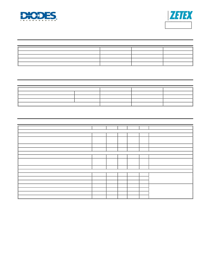
�Maximum� Ratings� @T� A� =� 25°C� unless� otherwise� specified�
�Characteristic�
�Drain-Source� Voltage�
�Gate-Source� Voltage�
�Continuous� Drain� Current�
�Pulsed� Drain� Current� (Note� 3)�
�Symbol�
�V� DSS�
�V� GSS�
�I� D�
�I� DM�
�Value�
�100�
�±20�
�1.67�
�12�
�Unit�
�V�
�V�
�A�
�A�
�Thermal� Characteristics� @T� A� =� 25°C� unless� otherwise� specified�
�Characteristic�
�Symbol�
�Value�
�Unit�
�Power� Dissipation�
�Thermal� Resistance,� Junction� to� Ambient�
�Thermal� Resistance,� Junction� to� Leads�
�Operating� and� Storage� Temperature� Range�
�(Note� 2)�
�(Note� 2)�
�(Note� 4)�
�P� D�
�R� θ� JA�
�R� θ� JL�
�T� J� ,� T� STG�
�3�
�41.7�
�8.84�
�-55� to� +150�
�W�
�°C/W�
�°C/W�
�°C�
�Electrical� Characteristics� @T� A� =� 25°C� unless� otherwise� specified�
�Characteristic�
�Symbol�
�Min�
�Typ�
�Max�
�Unit�
�Test� Condition�
�OFF� CHARACTERISTICS� (Note� 5)�
�Drain-Source� Breakdown� Voltage�
�Zero� Gate� Voltage� Drain� Current� T� J� =� 25°C�
�Gate-Source� Leakage�
�On-State� Drain� Current�
�BV� DSS�
�I� DSS�
�I� GSS�
�I� D(on)�
�100�
�-�
�-�
�9�
�-�
�-�
�-�
�-�
�-�
�10�
�100�
�±20�
�-�
�V�
�μA�
�μA�
�nA�
�A�
�V� GS� =� 0V,� I� D� =� 1mA�
�V� DS� =� 100V,� V� GS� =� 0V�
�V� DS� =� 80V,� V� GS� =� 0V,� T� A� =� 125°C�
�V� GS� =� ±20V,� V� DS� =� 0V�
�V� GS� =� 10V,� V� DS� =� 10V�
�ON� CHARACTERISTICS� (Note� 5)�
�Gate� Threshold� Voltage�
�Static� Drain-Source� On-Resistance�
�Forward� Transconductance�
�V� GS(th)�
�R� DS� (on)�
�g� fs�
�1�
�-�
�0.6�
�-�
�0.4�
�0.5�
�-�
�3�
�0.54�
�0.75�
�-�
�V�
�Ω�
�S�
�V� DS� =� V� GS� ,� I� D� =� 1mA�
�V� GS� =� 10V,� I� D� =� 3.3A�
�V� GS� =� 5V,� I� D� =� 1.5A�
�V� DS� =� 10V,� I� D� =� 3.3A�
�DYNAMIC� CHARACTERISTICS� (Note� 5)�
�Input� Capacitance�
�Output� Capacitance�
�Reverse� Transfer� Capacitance�
�Turn-On� Delay� Time�
�Turn-On� Rise� Time�
�Turn-Off� Delay� Time�
�Turn-Off� Fall� Time�
�C� iss�
�C� oss�
�C� rss�
�t� D(on)�
�t� r�
�t� D(off)�
�t� f�
�-�
�-�
�-�
�-�
�-�
�-�
�-�
�-�
�-�
�-�
�-�
�-�
�-�
�-�
�350�
�140�
�20�
�8�
�25�
�30�
�16�
�pF�
�pF�
�pF�
�ns�
�ns�
�ns�
�ns�
�V� DS� =� 25V,� V� GS� =� 0V,�
�f� =� 1.0MHz�
�V� DD� =� 25V,� I� D� =� 3A,� V� GEN� =� 10V,�
�R� GS� =� 50� ?�
�Notes:�
�2.� For� a� device� mounted� on� 50mm� X� 50mm� X� 1.6mm� FR-4� PCB� with� high� coverage� of� single� sided� 2oz� copper,� in� still� air� condition.�
�3.� Device� mounted� on� minimum� recommended� pad� layout� test� board,� 10� μ� s� pulse� duty� cycle� =� 1%.�
�4.� Thermal� resistance� from� junction� to� solder-point� (at� the� end� of� the� drain� lead).�
�5.� Short� duration� pulse� test� used� to� minimize� self-heating� effect.�
�ZVN4310G�
�Document� number:� DS33372� Rev.� 4� -� 2�
�2� of� 5�
�www.diodes.com�
�January� 2012�
�?� Diodes� Incorporated�
�相关PDF资料 |
PDF描述 |
|---|---|
| ZVN4424ASTOB | MOSFET N-CHAN 240V TO92-3 |
| ZVN4424GTC | MOSFET N-CHAN 240V SOT223 |
| ZVN4424ZTA | MOSFET N-CH 240V 300MA SOT-89 |
| ZVN4525E6TC | MOSFET N-CHAN 250V SOT23-6 |
| ZVN4525GTC | MOSFET N-CHAN 250V SOT223 |
相关代理商/技术参数 |
参数描述 |
|---|---|
| ZVN4424A | 功能描述:MOSFET N-Chnl 240V RoHS:否 制造商:STMicroelectronics 晶体管极性:N-Channel 汲极/源极击穿电压:650 V 闸/源击穿电压:25 V 漏极连续电流:130 A 电阻汲极/源极 RDS(导通):0.014 Ohms 配置:Single 最大工作温度: 安装风格:Through Hole 封装 / 箱体:Max247 封装:Tube |
| ZVN4424A | 制造商:Diodes Incorporated 功能描述:MOSFET N LOGIC E-LINE |
| ZVN4424ASTOA | 功能描述:MOSFET N-Chnl 240V RoHS:否 制造商:STMicroelectronics 晶体管极性:N-Channel 汲极/源极击穿电压:650 V 闸/源击穿电压:25 V 漏极连续电流:130 A 电阻汲极/源极 RDS(导通):0.014 Ohms 配置:Single 最大工作温度: 安装风格:Through Hole 封装 / 箱体:Max247 封装:Tube |
| ZVN4424ASTOB | 功能描述:MOSFET N-Chnl 240V RoHS:否 制造商:STMicroelectronics 晶体管极性:N-Channel 汲极/源极击穿电压:650 V 闸/源击穿电压:25 V 漏极连续电流:130 A 电阻汲极/源极 RDS(导通):0.014 Ohms 配置:Single 最大工作温度: 安装风格:Through Hole 封装 / 箱体:Max247 封装:Tube |
| ZVN4424ASTZ | 功能描述:MOSFET N-Chnl 240V RoHS:否 制造商:STMicroelectronics 晶体管极性:N-Channel 汲极/源极击穿电压:650 V 闸/源击穿电压:25 V 漏极连续电流:130 A 电阻汲极/源极 RDS(导通):0.014 Ohms 配置:Single 最大工作温度: 安装风格:Through Hole 封装 / 箱体:Max247 封装:Tube |
发布紧急采购,3分钟左右您将得到回复。