- 您现在的位置:买卖IC网 > PDF目录298413 > 5962-9960701TUX 512K X 8 STANDARD SRAM, 25 ns, CDFP36 PDF资料下载
参数资料
| 型号: | 5962-9960701TUX |
| 元件分类: | SRAM |
| 英文描述: | 512K X 8 STANDARD SRAM, 25 ns, CDFP36 |
| 封装: | BOTTOM BRAZED, CERAMIC, DFP-36 |
| 文件页数: | 8/15页 |
| 文件大小: | 121K |
| 代理商: | 5962-9960701TUX |
2
PIN NAMES
DEVICE OPERATION
The UT8Q512 has three control inputs called Enable 1 ( E), Write
Enable ( W), and Output Enable (G); 19 address inputs, A(18:0);
and eight bidirectional data lines, DQ(7:0). E Device Enable
controls device selection, active, and standby modes. Asserting
E enables the device, causes IDD to rise to its active value, and
decodes the 19 address inputs to select one of 524,288 words in
the memory. W controls read and write operations. During a
read cycle, G must be asserted to enable the outputs.
Table 1. Device Operation Truth Table
Notes:
1. “X” is defined as a “don’t care” condition.
2. Device active; outputs disabled.
READ CYCLE
A combination of W greater than V
IH (min) and E less than V IL
(max) defines a read cycle. Read access time is measured from
the latter of Device Enable, Output Enable, or valid address to
valid data output.
SRAM Read Cycle 1, the Address Access in figure 3a, is
initiated by a change in address inputs while the chip is enabled
with G asserted and W deasserted. Valid data appears on data
outputs DQ(7:0) after the specified t
AVQV is satisfied. Outputs
remain active throughout the entire cycle. As long as Device
Enable and Output Enable are active, the address inputs may
change at a rate equal to the minimum read cycle time (tAVAV).
SRAM read Cycle 2, the Chip Enable - Controlled Access in
figure 3b, is initiated by E going active while G remains asserted,
W remains deasserted, and the addresses remain stable for the
entire cycle. After the specified t
ETQV is satisfied, the eight-bit
word addressed by A(18:0) is accessed and appears at the data
outputs DQ(7:0).
SRAM read Cycle 3, the Output Enable - Controlled Access in
figure 3c, is initiated by G going active while E is asserted, W
is deasserted, and the addresses are stable. Read access time is
tGLQV unless tAVQV or tETQV have not been satisfied.
A(18:0)
Address
DQ(7:0)
Data Input/Output
E
Enable
W
Write Enable
G
Output Enable
VDD
Power
V
SS
Ground
1
36
2
35
3
34
4
33
5
32
6
31
7
30
8
29
9
28
10
27
11
26
12
25
13
24
14
23
15
22
16
21
17
20
18
19
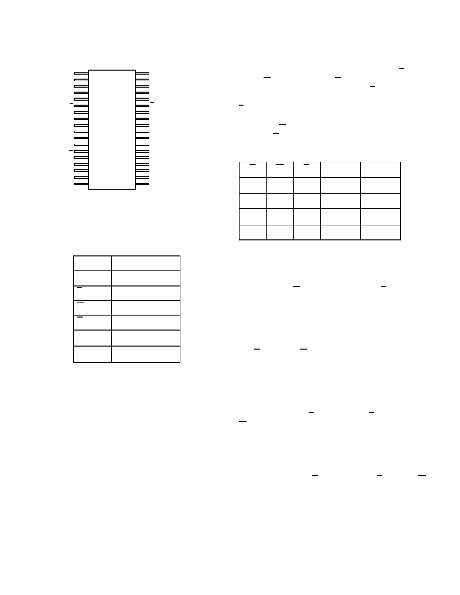
Figure 2. 25ns SRAM Pinout (36)
NC
A18
A17
A16
A15
G
DQ7
DQ6
VSS
VDD
DQ5
DQ4
A14
A13
A12
A11
A10
NC
A0
A1
A2
A3
A4
E
DQ0
DQ1
VDD
VSS
DQ2
DQ3
W
A5
A6
A7
A8
A9
G
W
E
I/O Mode
Mode
X1
X
1
3-state
Standby
X
0
Data in
Write
1
0
3-state
Read2
0
1
0
Data out
Read
相关PDF资料 |
PDF描述 |
|---|---|
| 5962-9960702QXA | 512K X 8 STANDARD SRAM, 25 ns, CDFP36 |
| 5962D0153301QXX | 512K X 32 MULTI DEVICE SRAM MODULE, 35 ns, QMA68 |
| 5962F0151601VYA | 8K X 8 OTPROM, 55 ns, CDFP28 |
| 5962F0323601QXX | 128K X 32 STANDARD SRAM, 15 ns, CQFP68 |
| 5962F9565802VCC | ACT SERIES, TRIPLE 3-INPUT NAND GATE, CDIP14 |
相关代理商/技术参数 |
参数描述 |
|---|---|
| 5962-9960801HUA | 制造商:International Rectifier 功能描述:Module DC-DC 1-OUT 5V 16A 80W 12-Pin AFL 制造商:International Rectifier 功能描述:DC TO DC CONVERTER 120 TO 5VDC 80W - Rail/Tube |
| 5962-9960901HZC | 制造商:International Rectifier 功能描述:MICROCIRCUIT, HYBRID, |
| 5962-9961001HXA | 功能描述:模数转换器 - ADC Dual 12 Bit105 MSPS MCM RoHS:否 制造商:Analog Devices 通道数量: 结构: 转换速率: 分辨率: 输入类型: 信噪比: 接口类型: 工作电源电压: 最大工作温度: 安装风格: 封装 / 箱体: |
| 5962-9961002HXA | 制造商:Analog Devices 功能描述:ADC Dual Pipelined 105Msps 12-bit Parallel 68-Pin CLCC 制造商:Analog Devices 功能描述:ADC DUAL PIPELINED 105MSPS 12-BIT PARALLEL 68CLCC - Bulk 制造商:Analog Devices Inc. 功能描述:Analog to Digital Converters - ADC Dual 12 Bit 105 MSPS A/D Converter MCM 制造商:Analog Devices Inc. 功能描述:Analog to Digital Converters - ADC Dual 12 Bit105 MSPS MCM 制造商:Analog Devices 功能描述:CONVERTER - ADC |
| 5962-9961502QYA | 制造商:e2v Aerospace & Defense 功能描述:Trans JFET N-CH 3-Pin TO-206AA 制造商:e2v Aerospace & Defense 功能描述:MEMORY, 64K X 9 CASCADABLE FIFO, 15 NS ACCESS TIME |
发布紧急采购,3分钟左右您将得到回复。