- 您现在的位置:买卖IC网 > PDF目录298413 > 5962F0323601QXX 128K X 32 STANDARD SRAM, 15 ns, CQFP68 PDF资料下载
参数资料
| 型号: | 5962F0323601QXX |
| 元件分类: | SRAM |
| 英文描述: | 128K X 32 STANDARD SRAM, 15 ns, CQFP68 |
| 封装: | CERAMIC, QFP-68 |
| 文件页数: | 10/16页 |
| 文件大小: | 297K |
| 代理商: | 5962F0323601QXX |

3
READ CYCLE
A combination of W and E2 greater than VIH (min) and E1 less
than VIL (max) defines a read cycle. Read access time is
measured from the latter of device enable, output enable, or
valid address to valid data output.
SRAM Read Cycle 1, the Address Access in Figure 3a, is
initiated by a change in address inputs while the chip is enabled
with G asserted and W deasserted. Valid data appears on data
outputs DQ(31:0) after the specified tAVQV is satisfied. Outputs
remain active throughout the entire cycle. As long as device
enable and output enable are active, the address inputs may
change at a rate equal to the minimum read cycle time (tAVAV).
SRAM Read Cycle 2, the Chip Enable-controlled Access in
Figure 3b, is initiated by the latter of E1 and E2 going active
while G remains asserted, W remains deasserted, and the
addresses remain stable for the entire cycle. After the specified
tETQV is satisfied, the 32-bit word addressed by A(16:0) is
accessed and appears at the data outputs DQ(31:0).
SRAM Read Cycle 3, the Output Enable-controlled Access in
Figure 3c, is initiated by G going active while E1 and E2 are
asserted, W is deasserted, and the addresses are stable. Read
access time is tGLQV unless tAVQV or tETQV have not been
satisfied.
Write Cycle
A combination of W and E1 less than VIL(max) and E2 greater
than VIH(min) defines a write cycle. The state of G is a “don’t
care” for a write cycle. The outputs are placed in the high-
impedance state when either G is greater than VIH(min), or
when W is less than VIL(max).
Write Cycle 1, the Write Enable-controlled Access in Figure
4a, is defined by a write terminated by W going high, with E1
and E2 still active. The write pulse width is defined by tWLWH
when the write is initiated by W, and by tETWH when the write
is initiated by E1 or E2. Unless the outputs have been
previously placed in the high-impedance state by G, the user
must wait user must wait tWLQZ before applying data to the 32
bidirectional pins DQ(31:0) to avoid bus contention.
Write Cycle 2, the Chip Enable-controlled Access in Figure 4b,
is defined by a write terminated by the latter of E1 or E2 going
inactive. The write pulse width is defined by tWLEF when the
write is initiated by W, and by tETEF when the write is initiated
by either E1or E2 going active. For the W initiated write, unless
the outputs have been previously placed in the high-impedance
state by G, the user must wait tWLQZ before applying data to
the sixteen bidirectional pins DQ(31:0) to avoid bus
contention.
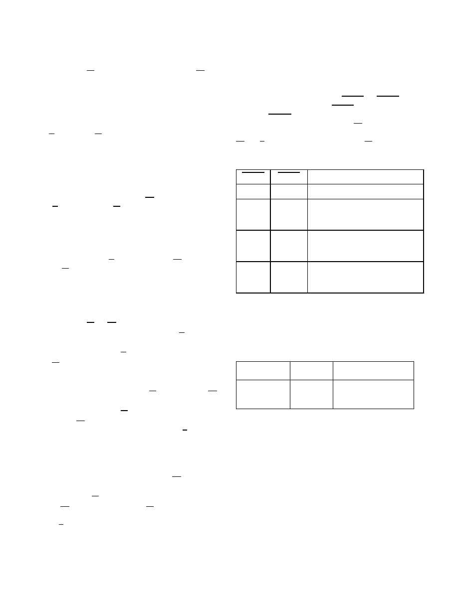
WORD ENABLES
Separate half-word enable controls (LHWE and HHWE) allow
individual 16-bit word accesses. LHWE controls the lower bits
DQ(15:0). HHWE controls the upper bits DQ(31:16). Writing
to the device is performed by asserting E1, E2 and the half-
word enables. Reading the device is performed by asserting
E1, E2, G, and the half-word enables while W is held inactive
(HIGH).
RADIATION HARDNESS
The UT8R128K32 SRAM incorporates special design, layout,
and process features which allows operation in a limited
radiation environment.
Table 2. Radiation Hardness Design Specifications1
Notes:
1. The SRAM is immune to latchup to particles >100MeV-cm2/mg.
2. 10% worst case particle environment, Geosynchronous orbit, 100 mils of
Aluminum.
Supply Sequencing
No supply voltage sequencing is required between VDD1 and
VDD2.
HHWE
LHWE
OPERATION
0
32-bit read or write cycle
0
1
16-bit high half-word read or write
cycle (low half-word bi-direction
pins DQ(15:0) are in 3 -state)
1
0
16-bit low half-word read or write
cycle (high half-word bi-direction
pins DQ(31:16) are in 3 -state)
1
High and low half-word bi-
directional pins remain in 3-state,
write function disabled
Total Dose
300K
rad(Si)
Heavy Ion
Error Rate2
8.9x10⁻¹⁰
Errors/Bit-Day
相关PDF资料 |
PDF描述 |
|---|---|
| 5962F9565802VCC | ACT SERIES, TRIPLE 3-INPUT NAND GATE, CDIP14 |
| ACTS10HMSR | ACT SERIES, TRIPLE 3-INPUT NAND GATE, UUC16 |
| 5962F9654202QXC | AC SERIES, QUAD 2-INPUT NAND GATE, CDFP14 |
| 5962F9654203QXC | AC SERIES, QUAD 2-INPUT NAND GATE, CDFP14 |
| 5962F9654203VXA | AC SERIES, QUAD 2-INPUT NAND GATE, CDFP14 |
相关代理商/技术参数 |
参数描述 |
|---|---|
| 5962F0521201VXC | 制造商:STMicroelectronics 功能描述:16-BIT EDGE-TRIGGERED D-TYPE FLIP-FLO- W/BUS HOLD, 3.3 VOLT. - Bulk |
| 5962F1023501KXA | 制造商:International Rectifier 功能描述:RAD HARD ULDO - Bulk |
| 5962F1023502K4A | 制造商:International Rectifier 功能描述:RAD HARD ULDO - Bulk |
| 5962F1023502K5A | 制造商:International Rectifier 功能描述:RAD HARD ULDO - Bulk |
| 5962F1023502K6A | 制造商:International Rectifier 功能描述:RAD HARD ULDO - Bulk |
发布紧急采购,3分钟左右您将得到回复。