- 您现在的位置:买卖IC网 > PDF目录294088 > 70V34S20PFGI (INTEGRATED DEVICE TECHNOLOGY INC) 4K X 18 DUAL-PORT SRAM, 20 ns, PQFP100 PDF资料下载
参数资料
| 型号: | 70V34S20PFGI |
| 厂商: | INTEGRATED DEVICE TECHNOLOGY INC |
| 元件分类: | SRAM |
| 英文描述: | 4K X 18 DUAL-PORT SRAM, 20 ns, PQFP100 |
| 封装: | 14 X 14 MM, 1.40 MM HEIGHT, GREEN, PLASTIC, TQFP-100 |
| 文件页数: | 2/25页 |
| 文件大小: | 211K |
| 代理商: | 70V34S20PFGI |
6.42
IDT70V35/34S/L
(IDT70V25/24S/L)
High-Speed 3.3V 8/4K x 18 (8/4K x 16) Dual-Port Static RAM
Industrial and Commercial Temperature Ranges
10
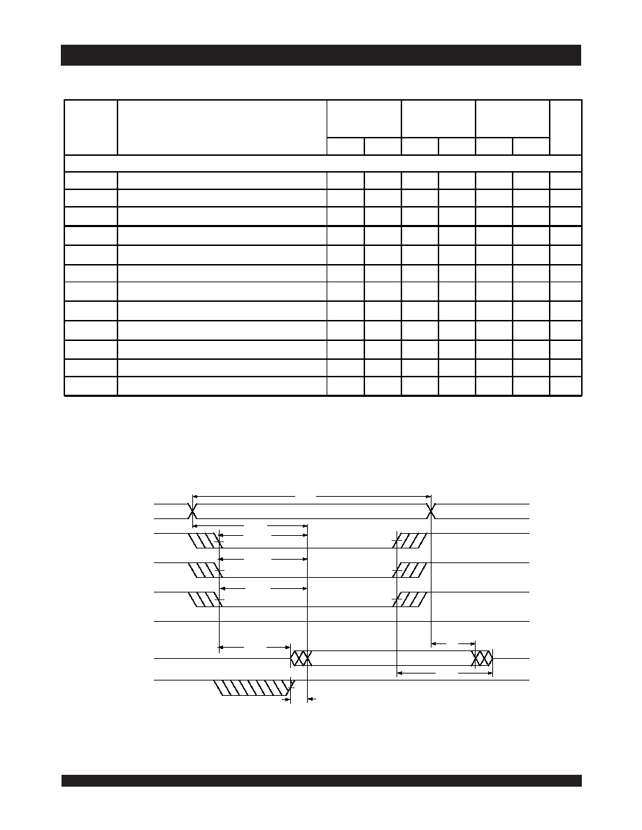
Waveform of Read Cycles(5)
NOTES:
1. Timing depends on which signal is asserted last,
OE, CE, LB, or UB.
2. Timing depends on which signal is de-asserted first,
CE, OE, LB, or UB.
3. tBDD delay is required only in case where opposite port is completing a write operation to the same address location for simultaneous read operations
BUSY
has no relation to valid output data.
4. Start of valid data depends on which timing becomes effective last tABE
, tAOE, tACE, tAA or tBDD.
5.
SEM = VIH.
tRC
R/
W
CE
ADDR
tAA
OE
UB, LB
5624 drw 08
(4)
tACE
(4)
tAOE
(4)
tABE
(4)
(1)
tLZ
tOH
(2)
tHZ
(3,4)
tBDD
DATAOUT
BUSYOUT
VALID DATA
(4)
AC Electrical Characteristics Over the Operating
Temperature and Supply Voltage Range for 70V35/34(4)
NOTES:
1. Transition is measured 0mV from Low or High-impedance voltage with Output Test Load (Figure 2).
2. This parameter is guaranteed by device characterization, but is not production tested.
3. To access RAM,
CE = VIL, UB or LB = VIL, and SEM = VIH. To access semaphore, CE = VIH or UB & LB = VIH, and SEM = VIL.
4. 'X' in part number indicates power rating (S or L).
70V35/34X15
Com'l Only
70V35/34X20
Com'l
& Ind
70V35/34X25
Com'l Only
Unit
Symbol
Parameter
Min.Max.Min.Max.Min.Max.
READ CYCLE
tRC
Read Cycle Time
15
____
20
____
25
____
ns
tAA
Address Access Time
____
15
____
20
____
25
ns
tACE
Chip Enable Access Time(3)
____
15
____
20
____
25
ns
tABE
Byte Enable Access Time(3)
____
15
____
20
____
25
ns
tAOE
Output Enable Access Time(3)
____
10
____
12
____
13
ns
tOH
Output Hold from Address Change
3
____
3
____
3
____
ns
tLZ
Output Low-Z Time
(1,2)
3
____
3
____
3
____
ns
tHZ
Output High-Z Time(1,2)
____
10
____
12
____
15
ns
tPU
Chip Enable to Power Up Time (1,2)
0
____
0
____
0
____
ns
tPD
Chip Disable to Power Down Time(1,2)
____
15
____
20
____
25
ns
tSOP
Semaphore Flag Update Pulse (
OE or SEM)10
____
10
____
10
____
ns
tSAA
Semaphore Address Access(3)
____
15
____
20
____
25
ns
5624 tbl 11
相关PDF资料 |
PDF描述 |
|---|---|
| 710-405J12 | STEEL, CIRCULAR ADAPTER |
| 710-405J16 | STEEL, CIRCULAR ADAPTER |
| 710-405J24 | STEEL, CIRCULAR ADAPTER |
| 710-405J32 | STEEL, CIRCULAR ADAPTER |
| 710-405J40 | STEEL, CIRCULAR ADAPTER |
相关代理商/技术参数 |
参数描述 |
|---|---|
| 70V34S25PF | 功能描述:静态随机存取存储器 RoHS:否 制造商:Cypress Semiconductor 存储容量:16 Mbit 组织:1 M x 16 访问时间:55 ns 电源电压-最大:3.6 V 电源电压-最小:2.2 V 最大工作电流:22 uA 最大工作温度:+ 85 C 最小工作温度:- 40 C 安装风格:SMD/SMT 封装 / 箱体:TSOP-48 封装:Tray |
| 70V34S25PF8 | 功能描述:静态随机存取存储器 RoHS:否 制造商:Cypress Semiconductor 存储容量:16 Mbit 组织:1 M x 16 访问时间:55 ns 电源电压-最大:3.6 V 电源电压-最小:2.2 V 最大工作电流:22 uA 最大工作温度:+ 85 C 最小工作温度:- 40 C 安装风格:SMD/SMT 封装 / 箱体:TSOP-48 封装:Tray |
| 70V3569S4BC | 功能描述:静态随机存取存储器 RoHS:否 制造商:Cypress Semiconductor 存储容量:16 Mbit 组织:1 M x 16 访问时间:55 ns 电源电压-最大:3.6 V 电源电压-最小:2.2 V 最大工作电流:22 uA 最大工作温度:+ 85 C 最小工作温度:- 40 C 安装风格:SMD/SMT 封装 / 箱体:TSOP-48 封装:Tray |
| 70V3569S4BC8 | 制造商:Integrated Device Technology Inc 功能描述:SRAM Chip Sync Dual 3.3V 576K-Bit 16K x 36 4.2ns 256-Pin CABGA T/R 制造商:Integrated Device Technology Inc 功能描述:SRAM SYNC DUAL 3.3V 576KBIT 16KX36 4.2NS 256BGA - Tape and Reel |
| 70V3569S4BF | 功能描述:静态随机存取存储器 RoHS:否 制造商:Cypress Semiconductor 存储容量:16 Mbit 组织:1 M x 16 访问时间:55 ns 电源电压-最大:3.6 V 电源电压-最小:2.2 V 最大工作电流:22 uA 最大工作温度:+ 85 C 最小工作温度:- 40 C 安装风格:SMD/SMT 封装 / 箱体:TSOP-48 封装:Tray |
发布紧急采购,3分钟左右您将得到回复。