- 您现在的位置:买卖IC网 > PDF目录294088 > 70V34S20PFGI (INTEGRATED DEVICE TECHNOLOGY INC) 4K X 18 DUAL-PORT SRAM, 20 ns, PQFP100 PDF资料下载
参数资料
| 型号: | 70V34S20PFGI |
| 厂商: | INTEGRATED DEVICE TECHNOLOGY INC |
| 元件分类: | SRAM |
| 英文描述: | 4K X 18 DUAL-PORT SRAM, 20 ns, PQFP100 |
| 封装: | 14 X 14 MM, 1.40 MM HEIGHT, GREEN, PLASTIC, TQFP-100 |
| 文件页数: | 9/25页 |
| 文件大小: | 211K |
| 代理商: | 70V34S20PFGI |
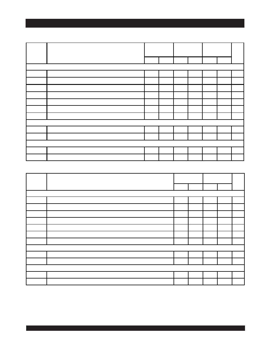
6.42
17
IDT70V35/34S/L (IDT70V25/24S/L)
High-Speed 3.3V 8/4K x 18 (8/4K x 16) Dual-Port Static RAM
Industrial and Commercial Temperature Ranges
AC Electrical Characteristics Over the Operating
Temperature and Supply Voltage Range for 70V25/24(6)
NOTES:
1. Port-to-port delay through SRAM cells from writing port to reading port, refer to "TIMING WAVEFORM OF WRITE PORT-TO-PORT READ AND
BUSY (M/S = VIH)".
2. To ensure that the earlier of the two ports wins.
3. tBDD is a calculated parameter and is the greater of 0, tWDD – tWP (actual) or tDDD – tDW (actual).
4. To ensure that the write cycle is inhibited during contention.
5. To ensure that a write cycle is completed after contention.
6. 'X' in part number indicates power rating (S or L).
70V25/24X15
Com'l Ony
70V25/24X20
Com'l
& Ind
70V25/24X25
Com'l
& Ind
Symbol
Parameter
Min.Max.Min.Max.Min.Max.
Unit
BUSY TIMING (M/S = VIH)
tBAA
BUSY Access Time from Address Match
____
15
____
20
____
20
ns
tBDA
BUSY Disable Time from Address Not Matched
____
15
____
20
____
20
ns
tBAC
BUSY Access Time from Chip Enable LOW
____
15
____
20
____
20
ns
tBDC
BUSY Disable Time from Chip Enable HIGH
____
15
____
17
____
17
ns
tAPS
Arbitration Priority Set-up Time
(2)
5
____
5
____
5
____
ns
tBDD
BUSY Disable to Valid Data(3)
____
18
____
30
____
30
ns
tWH
Write Hold After
BUSY(5)
12
____
15
____
17
____
ns
BUSY TIMING (M/S = VIL)
tWB
BUSY Input to Write(4)
0
____
0
____
0
____
ns
tWH
Write Hold After
BUSY(5)
12
____
15
____
17
____
ns
PORT-TO-PORT DELAY TIMING
tWDD
Write Pulse to Data Delay
(1)
____
30
____
45
____
50
ns
tDDD
Write Data Valid to Read Data Delay
(1)
____
25
____
35
____
35
ns
5624 tbl 13a
70V25/24X35
Com'l Only
70V25/24X55
Com'l Only
Symbol
Parameter
Min.
Max.
Min.
Max.
Unit
BUSY TIMING (M/S = VIH)
tBAA
BUSY Access Time from Address Match
____
20
____
45
ns
tBDA
BUSY Disable Time from Address Not Matched
____
20
____
40
ns
tBAC
BUSY Access Time from Chip Enable LOW
____
20
____
40
ns
tBDC
BUSY Disable Time from Chip Enable HIGH
____
20
____
35
ns
tAPS
Arbitration Priority Set-up Time
(2)
5
____
5
____
ns
tBDD
BUSY Disable to Valid Data(3)
____
35
____
40
ns
tWH
Write Hold After
BUSY(5)
25
____
25
____
ns
BUSY TIMING (M/S = VIL)
tWB
BUSY Input to Write(4)
0
____
0
____
ns
tWH
Write Hold After
BUSY(5)
25
____
25
____
ns
PORT-TO-PORT DELAY TIMING
tWDD
Write Pulse to Data Delay
(1)
____
60
____
80
ns
tDDD
Write Data Valid to Read Data Delay
(1)
____
45
____
65
ns
5624 tbl 13b
相关PDF资料 |
PDF描述 |
|---|---|
| 710-405J12 | STEEL, CIRCULAR ADAPTER |
| 710-405J16 | STEEL, CIRCULAR ADAPTER |
| 710-405J24 | STEEL, CIRCULAR ADAPTER |
| 710-405J32 | STEEL, CIRCULAR ADAPTER |
| 710-405J40 | STEEL, CIRCULAR ADAPTER |
相关代理商/技术参数 |
参数描述 |
|---|---|
| 70V34S25PF | 功能描述:静态随机存取存储器 RoHS:否 制造商:Cypress Semiconductor 存储容量:16 Mbit 组织:1 M x 16 访问时间:55 ns 电源电压-最大:3.6 V 电源电压-最小:2.2 V 最大工作电流:22 uA 最大工作温度:+ 85 C 最小工作温度:- 40 C 安装风格:SMD/SMT 封装 / 箱体:TSOP-48 封装:Tray |
| 70V34S25PF8 | 功能描述:静态随机存取存储器 RoHS:否 制造商:Cypress Semiconductor 存储容量:16 Mbit 组织:1 M x 16 访问时间:55 ns 电源电压-最大:3.6 V 电源电压-最小:2.2 V 最大工作电流:22 uA 最大工作温度:+ 85 C 最小工作温度:- 40 C 安装风格:SMD/SMT 封装 / 箱体:TSOP-48 封装:Tray |
| 70V3569S4BC | 功能描述:静态随机存取存储器 RoHS:否 制造商:Cypress Semiconductor 存储容量:16 Mbit 组织:1 M x 16 访问时间:55 ns 电源电压-最大:3.6 V 电源电压-最小:2.2 V 最大工作电流:22 uA 最大工作温度:+ 85 C 最小工作温度:- 40 C 安装风格:SMD/SMT 封装 / 箱体:TSOP-48 封装:Tray |
| 70V3569S4BC8 | 制造商:Integrated Device Technology Inc 功能描述:SRAM Chip Sync Dual 3.3V 576K-Bit 16K x 36 4.2ns 256-Pin CABGA T/R 制造商:Integrated Device Technology Inc 功能描述:SRAM SYNC DUAL 3.3V 576KBIT 16KX36 4.2NS 256BGA - Tape and Reel |
| 70V3569S4BF | 功能描述:静态随机存取存储器 RoHS:否 制造商:Cypress Semiconductor 存储容量:16 Mbit 组织:1 M x 16 访问时间:55 ns 电源电压-最大:3.6 V 电源电压-最小:2.2 V 最大工作电流:22 uA 最大工作温度:+ 85 C 最小工作温度:- 40 C 安装风格:SMD/SMT 封装 / 箱体:TSOP-48 封装:Tray |
发布紧急采购,3分钟左右您将得到回复。