- 您现在的位置:买卖IC网 > PDF目录16263 > 73S1215F-EB (Maxim Integrated Products)BOARD EVAL 73S1215F CBL/DOC/CD PDF资料下载
参数资料
| 型号: | 73S1215F-EB |
| 厂商: | Maxim Integrated Products |
| 文件页数: | 13/136页 |
| 文件大小: | 0K |
| 描述: | BOARD EVAL 73S1215F CBL/DOC/CD |
| 产品培训模块: | Lead (SnPb) Finish for COTS Obsolescence Mitigation Program |
| 标准包装: | 1 |
| 系列: | * |
第1页第2页第3页第4页第5页第6页第7页第8页第9页第10页第11页第12页当前第13页第14页第15页第16页第17页第18页第19页第20页第21页第22页第23页第24页第25页第26页第27页第28页第29页第30页第31页第32页第33页第34页第35页第36页第37页第38页第39页第40页第41页第42页第43页第44页第45页第46页第47页第48页第49页第50页第51页第52页第53页第54页第55页第56页第57页第58页第59页第60页第61页第62页第63页第64页第65页第66页第67页第68页第69页第70页第71页第72页第73页第74页第75页第76页第77页第78页第79页第80页第81页第82页第83页第84页第85页第86页第87页第88页第89页第90页第91页第92页第93页第94页第95页第96页第97页第98页第99页第100页第101页第102页第103页第104页第105页第106页第107页第108页第109页第110页第111页第112页第113页第114页第115页第116页第117页第118页第119页第120页第121页第122页第123页第124页第125页第126页第127页第128页第129页第130页第131页第132页第133页第134页第135页第136页
DS_1215F_003
73S1215F Data Sheet
Rev. 1.4
11
1.2 Hardware Overview
The Teridian 73S1215F single smart card controller integrates all primary functional blocks required to
implement a smart card reader. Included on chip are an 8051-compatible microprocessor (MPU) which
executes up to one instruction per clock cycle (80515), a fully integrated IS0-7816 compliant smart card
interface, expansion smart card interface, full speed USB 2.0 compatible interface, serial interface, I2C
interface, 6 x 5 keypad interface, 4 LED drivers, RAM, FLASH memory, a real time clock (RTC), and a
variety of I/O pins. Figure 1 shows a functional block diagram of the 73S1215F.
1.3 80515 MPU Core
1.3.1 80515 Overview
The 73S1215F includes an 80515 MPU (8-bit, 8051-compatible) that performs most instructions in one
clock cycle. The 80515 architecture eliminates redundant bus states and implements parallel execution
of fetch and execution phases. Normally a machine cycle is aligned with a memory fetch, therefore, most
of the 1-byte instructions are performed in a single cycle. This leads to an 8x performance (average)
improvement (in terms of MIPS) over the Intel 8051 device running at the same clock frequency.
Actual processor clocking speed can be adjusted to the total processing demand of the application
(cryptographic calculations, key management, memory management, and I/O management) using the
XRAM special function register MPUCKCtl.
Typical smart card, USB, serial, keyboard, I2C, and RTC management functions are available for the
MPU as part of the Teridian standard library. A standard ANSI “C” 80515-application programming
interface library is available to help reduce design cycle. Refer to the 73S12xxF Software User’s Guide.
1.3.2 Memory Organization
The 80515 MPU core incorporates the Harvard architecture with separate code and data spaces.
Memory organization in the 80515 is similar to that of the industry standard 8051. There are three
memory areas: Program memory (Flash), external data memory (XRAM), and internal data memory
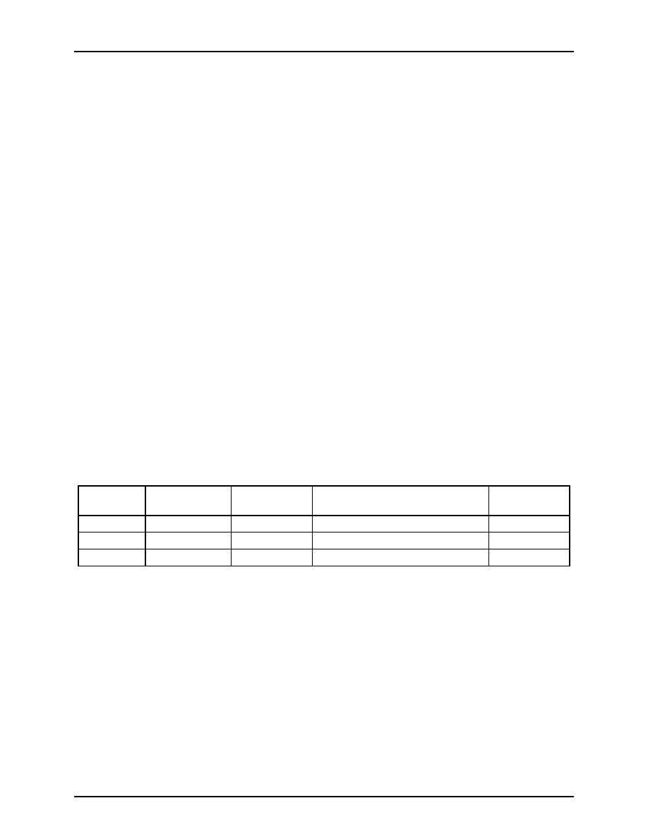
(IRAM). Data bus address space is allocated to on-chip memory as shown Table 2.
Table 2: MPU Data Memory Map
Address
(hex)
Memory
Technology
Memory Type
Typical Usage
Memory Size
(bytes)
0000-FFFF
Flash Memory
Non-volatile
Program and non-volatile data
64KB
0000-07FF
Static RAM
Volatile
MPU data XRAM
2KB
FC00-FFFF External SFR
Volatile
Peripheral control
1KB
Note: The IRAM is part of the core and is addressed differently.
Program Memory: The 80515 can address up to 64KB of program memory space from 0x0000 to
0xFFFF. Program memory is read when the MPU fetches instructions or performs a MOVC operation.
After reset, the MPU starts program execution from location 0x0000. The lower part of the program
memory includes reset and interrupt vectors. The interrupt vectors are spaced at 8-byte intervals, starting
from 0x0003 (Reset is located at 0x0000).
Flash Memory: The program memory consists of flash memory. The flash memory is intended to
primarily contain MPU program code. Flash erasure is initiated by writing a specific data pattern to
specific SFR registers in the proper sequence. These special pattern/sequence requirements prevent
inadvertent erasure of the flash memory.
相关PDF资料 |
PDF描述 |
|---|---|
| ECC22DCST | CONN EDGECARD 44POS DIP .100 SLD |
| 73S1210F-EB | BOARD EVAL 73S1210F DOC/CD CABLE |
| ECC22DCMT | CONN EDGECARD 44POS .100 WW |
| 73S1209F-EB | BOARD EVAL 73S1209F DOC/CD CABLE |
| EBC25DTAS | CONN EDGECARD 50POS R/A .100 SLD |
相关代理商/技术参数 |
参数描述 |
|---|---|
| 73S1215F-EB-Lite | 功能描述:开发板和工具包 - 8051 73S1215F Eval Brd Lite (USD Cbl, D.Cd) RoHS:否 制造商:Silicon Labs 产品:Development Kits 工具用于评估:C8051F960, Si7005 核心: 接口类型:USB 工作电源电压: |
| 73S1217F | 制造商:TERIDIAN 制造商全称:TERIDIAN 功能描述:Bus-Powered 80515 System-on-Chip with USB, ISO 7816 / EMV, PINpad and More |
| 73S1217F-68IM/F | 功能描述:8位微控制器 -MCU Bus Pwr’d 80515 SoC w/USB 7816/EMV PINpd RoHS:否 制造商:Silicon Labs 核心:8051 处理器系列:C8051F39x 数据总线宽度:8 bit 最大时钟频率:50 MHz 程序存储器大小:16 KB 数据 RAM 大小:1 KB 片上 ADC:Yes 工作电源电压:1.8 V to 3.6 V 工作温度范围:- 40 C to + 105 C 封装 / 箱体:QFN-20 安装风格:SMD/SMT |
| 73S1217F-68IM/F/P | 功能描述:IC SMART CARD READER PROG 68-QFN RoHS:是 类别:集成电路 (IC) >> 嵌入式 - 微控制器, 系列:73S12xx 产品培训模块:MCU Product Line Introduction AVR® UC3 Introduction 标准包装:2,500 系列:AVR®32 UC3 B 核心处理器:AVR 芯体尺寸:32-位 速度:60MHz 连通性:I²C,IrDA,SPI,SSC,UART/USART,USB 外围设备:欠压检测/复位,DMA,POR,PWM,WDT 输入/输出数:28 程序存储器容量:128KB(128K x 8) 程序存储器类型:闪存 EEPROM 大小:- RAM 容量:32K x 8 电压 - 电源 (Vcc/Vdd):1.65 V ~ 1.95 V 数据转换器:A/D 6x10b 振荡器型:内部 工作温度:-40°C ~ 85°C 封装/外壳:48-TQFP 包装:带卷 (TR) 配用:ATSTK600-TQFP48-ND - STK600 SOCKET/ADAPTER 48-TQFPATAVRONEKIT-ND - KIT AVR/AVR32 DEBUGGER/PROGRMMRATEVK1101-ND - KIT DEV/EVAL FOR AVR32 AT32UC3B 其它名称:AT32UC3B1128-AUR-NDAT32UC3B1128-AURTR |
| 73S1217F-68IMR/F | 功能描述:8位微控制器 -MCU Bus Pwr’d 80515 SoC w/USB 7816/EMV PINpd RoHS:否 制造商:Silicon Labs 核心:8051 处理器系列:C8051F39x 数据总线宽度:8 bit 最大时钟频率:50 MHz 程序存储器大小:16 KB 数据 RAM 大小:1 KB 片上 ADC:Yes 工作电源电压:1.8 V to 3.6 V 工作温度范围:- 40 C to + 105 C 封装 / 箱体:QFN-20 安装风格:SMD/SMT |
发布紧急采购,3分钟左右您将得到回复。