- 您现在的位置:买卖IC网 > PDF目录15272 > LTC1909-8EG (Linear Technology)IC REG CTRLR BUCK PWM CM 28-SSOP PDF资料下载
参数资料
| 型号: | LTC1909-8EG |
| 厂商: | Linear Technology |
| 文件页数: | 10/32页 |
| 文件大小: | 0K |
| 描述: | IC REG CTRLR BUCK PWM CM 28-SSOP |
| 标准包装: | 47 |
| PWM 型: | 电流模式 |
| 输出数: | 1 |
| 频率 - 最大: | 200kHz |
| 占空比: | 90% |
| 电源电压: | 4 V ~ 36 V |
| 降压: | 是 |
| 升压: | 无 |
| 回扫: | 无 |
| 反相: | 无 |
| 倍增器: | 无 |
| 除法器: | 无 |
| Cuk: | 无 |
| 隔离: | 无 |
| 工作温度: | -40°C ~ 85°C |
| 封装/外壳: | 28-SSOP(0.209",5.30mm 宽) |
| 包装: | 管件 |
| 其它名称: | LTC19098EG |
第1页第2页第3页第4页第5页第6页第7页第8页第9页当前第10页第11页第12页第13页第14页第15页第16页第17页第18页第19页第20页第21页第22页第23页第24页第25页第26页第27页第28页第29页第30页第31页第32页
�� �
�
�LTC1909-8�
�PI� FU� CTIO� S�
�FB� (Pin� 17):� Feedback� Input.� Center� tap� of� the� SMBus�
�programmable� divider� that� is� connected� to� Pin� 9.�
�GND� (Pin� 18):� SMBus� Programmer� Ground.� Connect� to�
�regulator� signal� ground� at� Pin� 7.�
�V� CC� (Pin� 19):� Positive� Supply� of� the� SMBus� VID� Program-�
�mer.� 2.7V� ≤� V� CC� ≤� 5.5V.� May� be� connected� to� the� INTV� CC�
�pin.� Bypass� this� pin� to� ground� with� a� 0.1� μ� F� ceramic�
�capacitor� if� using� an� external� supply.�
�EXTV� CC� (Pin� 20):� External� V� CC� Input.� When� EXTV� CC� ex-�
�ceeds� 4.7V,� an� internal� switch� connects� this� pin� to� INTV� CC�
�and� shuts� down� the� internal� regulator� so� that� controller�
�and� gate� drive� power� is� drawn� from� EXTV� CC� .� Do� not� exceed�
�7V� at� this� pin� and� ensure� that� EXTV� CC� <� V� IN� .�
�V� IN� (Pin� 21):� Main� Input� Supply.� Decouple� this� pin� to�
�PGND� with� an� RC� filter� (1� ?� ,� 0.1� μ� F).�
�INTV� CC� (Pin� 22):� Internal� 5V� Regulator� Output.� The� driver�
�and� control� circuits� are� powered� from� this� voltage.� De-�
�couple� this� pin� to� power� ground� with� a� minimum� of� 4.7� μ� F�
�low� ESR� tantalum� or� other� low� ESR� capacitor.� The� internal�
�BG� (Pin� 23):� Bottom� Gate� Drive.� Drives� the� gate� of� the�
�bottom� N-channel� MOSFET� between� ground� and� INTV� CC� .�
�PGND� (Pin� 24):� Power� Ground.� Connect� this� pin� closely� to�
�the� source� of� the� bottom� N-channel� MOSFET,� the� (–)�
�terminal� of� C� VCC� and� the� (–)� terminal� of� C� IN� .�
�SENSE� +� (Pin� 25):� Current� Sense� Comparator� Input.� The�
�(+)� input� to� the� current� comparator� is� normally� connected�
�to� the� SW� pin� unless� using� a� sense� resistor� (see� Applica-�
�tions� Information).�
�SW� (Pin� 26):� Switch� Node.� The� (–)� terminal� of� the� boot-�
�strap� capacitor� C� B� connects� here.� This� pin� swings� from� a�
�diode� voltage� drop� below� ground� up� to� V� IN� .�
�TG� (Pin� 27):� Top� Gate� Drive.� Drives� the� top� N-channel�
�MOSFET� with� a� voltage� swing� equal� to� INTV� CC� superim-�
�posed� on� the� switch� node� voltage� SW.�
�BOOST� (Pin� 28):� Boosted� Floating� Driver� Supply.� The� (+)�
�terminal� of� the� bootstrap� capacitor� C� B� connects� here.� This�
�pin� swings� from� a� diode� voltage� drop� below� INTV� CC� up� to�
�V� IN� +� INTV� CC� .�
�5V� regulator� is� shut� down� when� V� RUN/SS� <1.5V.�
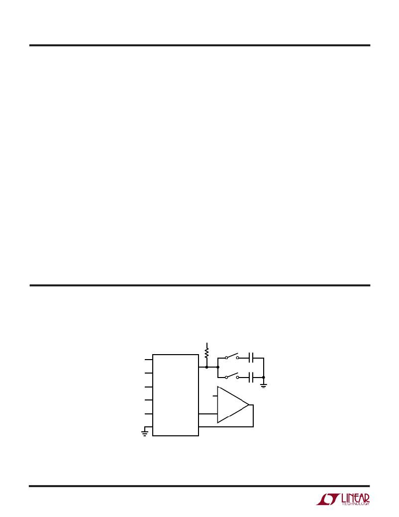
�TEST� CIRCUIT�
�SMBus� VID� Programmer� Test� Circuit�
�5V�
�10k�
�S1�
�0.1� μ� F�
�V� CC�
�V� CC�
�CPUON� OR�
�SCL�
�SCL�
�PGTMR�
�S2�
�100pF�
�SDA�
�SDA�
�SEL�
�VRON�
�SEL�
�VRON�
�GND�
�FB�
�V� OSENSE�
�0.8V�
�+�
�–�
�19098� TC�
�19098f�
�10�
�相关PDF资料 |
PDF描述 |
|---|---|
| H2BXG-10108-Y4-ND | JUMPER-H1501TR/A2015Y/X 8" |
| LTC1149CS-3.3#PBF | IC REG CTRLR BUCK PWM CM 16-SOIC |
| VI-JWB-EY-F2 | CONVERTER MOD DC/DC 95V 50W |
| VI-273-EW-F1 | CONVERTER MOD DC/DC 24V 100W |
| LTC3708EUH#TRPBF | IC REG CTRLR BUCK PWM CM 32-QFN |
相关代理商/技术参数 |
参数描述 |
|---|---|
| 74HC273DB | 功能描述:触发器 OCTAL D-TYPE RoHS:否 制造商:Texas Instruments 电路数量:2 逻辑系列:SN74 逻辑类型:D-Type Flip-Flop 极性:Inverting, Non-Inverting 输入类型:CMOS 输出类型: 传播延迟时间:4.4 ns 高电平输出电流:- 16 mA 低电平输出电流:16 mA 电源电压-最大:5.5 V 最大工作温度:+ 85 C 安装风格:SMD/SMT 封装 / 箱体:X2SON-8 封装:Reel |
| 74HC273DB,112 | 功能描述:触发器 OCTAL D-TYPE RoHS:否 制造商:Texas Instruments 电路数量:2 逻辑系列:SN74 逻辑类型:D-Type Flip-Flop 极性:Inverting, Non-Inverting 输入类型:CMOS 输出类型: 传播延迟时间:4.4 ns 高电平输出电流:- 16 mA 低电平输出电流:16 mA 电源电压-最大:5.5 V 最大工作温度:+ 85 C 安装风格:SMD/SMT 封装 / 箱体:X2SON-8 封装:Reel |
| 74HC273DB,118 | 功能描述:触发器 OCTAL D-TYPE RoHS:否 制造商:Texas Instruments 电路数量:2 逻辑系列:SN74 逻辑类型:D-Type Flip-Flop 极性:Inverting, Non-Inverting 输入类型:CMOS 输出类型: 传播延迟时间:4.4 ns 高电平输出电流:- 16 mA 低电平输出电流:16 mA 电源电压-最大:5.5 V 最大工作温度:+ 85 C 安装风格:SMD/SMT 封装 / 箱体:X2SON-8 封装:Reel |
| 74HC273DBT | 制造商:NXP Semiconductors 功能描述:HC/UH SERIES, POSITIVE EDGE TRIGGERED D FLIP-FLOP, TRUE OUTPUT, 20 Pin Plastic SMT |
| 74HC273DB-T | 功能描述:触发器 OCTAL D-TYPE RoHS:否 制造商:Texas Instruments 电路数量:2 逻辑系列:SN74 逻辑类型:D-Type Flip-Flop 极性:Inverting, Non-Inverting 输入类型:CMOS 输出类型: 传播延迟时间:4.4 ns 高电平输出电流:- 16 mA 低电平输出电流:16 mA 电源电压-最大:5.5 V 最大工作温度:+ 85 C 安装风格:SMD/SMT 封装 / 箱体:X2SON-8 封装:Reel |
发布紧急采购,3分钟左右您将得到回复。