- 您现在的位置:买卖IC网 > PDF目录15272 > LTC1909-8EG (Linear Technology)IC REG CTRLR BUCK PWM CM 28-SSOP PDF资料下载
参数资料
| 型号: | LTC1909-8EG |
| 厂商: | Linear Technology |
| 文件页数: | 23/32页 |
| 文件大小: | 0K |
| 描述: | IC REG CTRLR BUCK PWM CM 28-SSOP |
| 标准包装: | 47 |
| PWM 型: | 电流模式 |
| 输出数: | 1 |
| 频率 - 最大: | 200kHz |
| 占空比: | 90% |
| 电源电压: | 4 V ~ 36 V |
| 降压: | 是 |
| 升压: | 无 |
| 回扫: | 无 |
| 反相: | 无 |
| 倍增器: | 无 |
| 除法器: | 无 |
| Cuk: | 无 |
| 隔离: | 无 |
| 工作温度: | -40°C ~ 85°C |
| 封装/外壳: | 28-SSOP(0.209",5.30mm 宽) |
| 包装: | 管件 |
| 其它名称: | LTC19098EG |
第1页第2页第3页第4页第5页第6页第7页第8页第9页第10页第11页第12页第13页第14页第15页第16页第17页第18页第19页第20页第21页第22页当前第23页第24页第25页第26页第27页第28页第29页第30页第31页第32页
�� �
�
�LTC1909-8�
�APPLICATIO� S� I� FOR� ATIO�
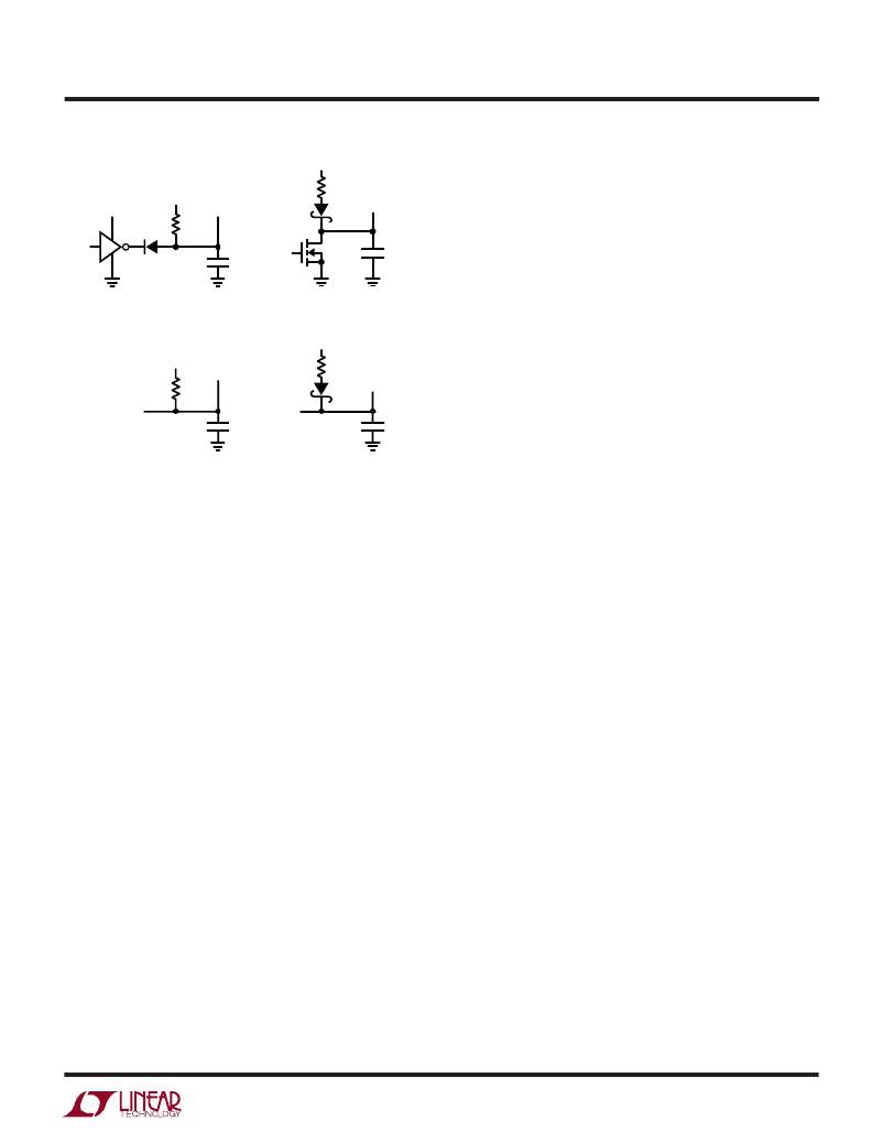
�INTV� CC�
�shown� in� Figure� 6a� or� 6c� is� simple,� but� slightly� increases�
�3.3V� OR� 5V�
�V� IN�
�RUN/SS�
�R� SS� *�
�D2*�
�RUN/SS�
�shutdown� current.� Connecting� a� resistor� to� INTV� CC� as�
�shown� in� Figure� 6b� and� 6d� eliminates� the� additional�
�D1�
�R� SS� *�
�shutdown� current,� but� requires� a� diode� to� isolate� C� SS� .� Any�
�C� SS�
�*OPTIONAL� TO� OVERRIDE� OVERCURRENT� LATCHOFF�
�C� SS�
�pull-up� network� must� be� able� to� maintain� RUN/SS� above�
�the� 4.2V� maximum� latchoff� threshold� and� overcome� the�
�4� μ� A� maximum� discharge� current.�
�(6a)�
�(6b)�
�Efficiency� Considerations�
�V� IN�
�RUN/SS�
�R� SS� *�
�INTV� CC�
�R� SS� *�
�D2*�
�RUN/SS�
�The� percent� efficiency� of� a� switching� regulator� is� equal� to�
�the� output� power� divided� by� the� input� power� times� 100%.�
�It� is� often� useful� to� analyze� individual� losses� to� determine�
�CPUON�
�C� SS�
�CPUON�
�C� SS�
�what� is� limiting� the� efficiency� and� which� change� would�
�produce� the� most� improvement.� Although� all� dissipative�
�19098� F06�
�*OPTIONAL� TO� OVERRIDE� OVERCURRENT� LATCHOFF�
�(6c)� (6d)�
�Figure� 6.� RUN/SS� Pin� Interfacing� with� Latchoff� Defeated�
�controller� turns� off� both� power� MOSFETs,� shutting� down�
�the� converter� permanently.� The� RUN/SS� pin� must� be�
�actively� pulled� down� to� ground� in� order� to� restart� opera-�
�tion.� If� the� RUN/SS� pin� is� tied� to� the� CPUON� pin,� this� is�
�achieved� by� pulling� the� VRON� pin� low� or� by� sending� two�
�Off� protocols� to� the� SMBus� VID� programmer� to� force� the�
�CPUON� pin� low.�
�The� overcurrent� protection� timer� requires� that� the� soft-�
�start� timing� capacitor� C� SS� be� made� large� enough� to� guar-�
�antee� that� the� output� is� in� regulation� by� the� time� C� SS� has�
�reached� the� 4V� threshold.� In� general,� this� will� depend� upon�
�the� size� of� the� output� capacitance,� output� voltage� and� load�
�current� characteristic.� A� minimum� soft-start� capacitor� can�
�be� estimated� from:�
�C� SS� >� C� OUT� V� OUT� R� SENSE� (10� –� 4� [F/V� s])�
�Generally� 0.1� μ� F� is� more� than� sufficient.�
�Overcurrent� latchoff� operation� is� not� always� needed� or�
�desired.� Load� current� is� already� limited� during� a� short-�
�circuit� by� the� current� foldback� circuitry� and� latchoff� opera-�
�tion� can� prove� annoying� during� troubleshooting.� The�
�feature� can� be� overridden� by� adding� a� pull-up� current�
�greater� than� 5� μ� A� to� the� RUN/SS� pin.� The� additional� current�
�prevents� the� discharge� of� C� SS� during� a� fault� and� also�
�shortens� the� soft-start� period.� Using� a� resistor� to� V� IN� as�
�elements� in� the� circuit� produce� losses,� four� main� sources�
�account� for� most� of� the� losses� in� LTC1909-8� circuits:�
�1.� DC� I� 2� R� losses.� These� arise� from� the� resistances� of� the�
�MOSFETs,� inductor� and� PC� board� traces� and� cause� the�
�efficiency� to� drop� at� high� output� currents.� In� continuous�
�mode� the� average� output� current� flows� through� L,� but� is�
�chopped� between� the� top� and� bottom� MOSFETs.� If� the� two�
�MOSFETs� have� approximately� the� same� R� DS(ON)� ,� then� the�
�resistance� of� one� MOSFET� can� simply� be� summed� with� the�
�resistances� of� L� and� the� board� traces� to� obtain� the� DC� I� 2� R�
�loss.� For� example,� if� R� DS(ON)� =� 0.01� ?� and� R� L� =� 0.005� ?� ,� the�
�loss� will� range� from� 15mW� to� 1.5W� as� the� output� current�
�varies� from� 1A� to� 10A.�
�2.� Transition� loss.� This� loss� arises� from� the� brief� amount�
�of� time� the� top� MOSFET� spends� in� the� saturated� region�
�during� switch� node� transitions.� It� depends� upon� the� input�
�voltage,� load� current,� driver� strength� and� MOSFET�
�capacitance,� among� other� factors.� The� loss� is� significant�
�at� input� voltages� above� 20V� and� can� be� estimated� from:�
�Transition� Loss� ?� (1.7A� –1� )� V� IN2� I� OUT� C� RSS� f�
�3.� INTV� CC� current.� This� is� the� sum� of� the� MOSFET� driver�
�and� control� currents.� This� loss� can� be� reduced� by� supply-�
�ing� INTV� CC� current� through� the� EXTV� CC� pin� from� a� high�
�efficiency� source,� such� as� an� output� derived� boost� net-�
�work� or� alternate� supply� if� available.�
�4.� C� IN� loss.� The� input� capacitor� has� the� difficult� job� of�
�filtering� the� large� RMS� input� current� to� the� regulator.� It�
�must� have� a� very� low� ESR� to� minimize� the� AC� I� 2� R� loss� and�
�19098f�
�23�
�相关PDF资料 |
PDF描述 |
|---|---|
| H2BXG-10108-Y4-ND | JUMPER-H1501TR/A2015Y/X 8" |
| LTC1149CS-3.3#PBF | IC REG CTRLR BUCK PWM CM 16-SOIC |
| VI-JWB-EY-F2 | CONVERTER MOD DC/DC 95V 50W |
| VI-273-EW-F1 | CONVERTER MOD DC/DC 24V 100W |
| LTC3708EUH#TRPBF | IC REG CTRLR BUCK PWM CM 32-QFN |
相关代理商/技术参数 |
参数描述 |
|---|---|
| LTC1909-8EG#PBF | 功能描述:IC REG CTRLR BUCK PWM CM 28-SSOP RoHS:是 类别:集成电路 (IC) >> PMIC - 稳压器 - DC DC 切换控制器 系列:- 标准包装:4,500 系列:PowerWise® PWM 型:控制器 输出数:1 频率 - 最大:1MHz 占空比:95% 电源电压:2.8 V ~ 5.5 V 降压:是 升压:无 回扫:无 反相:无 倍增器:无 除法器:无 Cuk:无 隔离:无 工作温度:-40°C ~ 125°C 封装/外壳:6-WDFN 裸露焊盘 包装:带卷 (TR) 配用:LM1771EVAL-ND - BOARD EVALUATION LM1771 其它名称:LM1771SSDX |
| LTC1909-8EG#TR | 功能描述:IC REG CTRLR BUCK PWM CM 28-SSOP RoHS:否 类别:集成电路 (IC) >> PMIC - 稳压器 - DC DC 切换控制器 系列:- 标准包装:4,500 系列:PowerWise® PWM 型:控制器 输出数:1 频率 - 最大:1MHz 占空比:95% 电源电压:2.8 V ~ 5.5 V 降压:是 升压:无 回扫:无 反相:无 倍增器:无 除法器:无 Cuk:无 隔离:无 工作温度:-40°C ~ 125°C 封装/外壳:6-WDFN 裸露焊盘 包装:带卷 (TR) 配用:LM1771EVAL-ND - BOARD EVALUATION LM1771 其它名称:LM1771SSDX |
| LTC1909-8EG#TRPBF | 功能描述:IC REG CTRLR BUCK PWM CM 28-SSOP RoHS:是 类别:集成电路 (IC) >> PMIC - 稳压器 - DC DC 切换控制器 系列:- 标准包装:4,500 系列:PowerWise® PWM 型:控制器 输出数:1 频率 - 最大:1MHz 占空比:95% 电源电压:2.8 V ~ 5.5 V 降压:是 升压:无 回扫:无 反相:无 倍增器:无 除法器:无 Cuk:无 隔离:无 工作温度:-40°C ~ 125°C 封装/外壳:6-WDFN 裸露焊盘 包装:带卷 (TR) 配用:LM1771EVAL-ND - BOARD EVALUATION LM1771 其它名称:LM1771SSDX |
| LTC1911EMS8-1.5#PBF | 功能描述:IC REG BUCK 1.5V 0.25A 8MSOP RoHS:是 类别:集成电路 (IC) >> PMIC - 稳压器 - DC DC 开关稳压器 系列:- 标准包装:2,500 系列:- 类型:升压(升压) 输出类型:可调式 输出数:1 输出电压:1.24 V ~ 30 V 输入电压:1.5 V ~ 12 V PWM 型:电流模式,混合 频率 - 开关:600kHz 电流 - 输出:500mA 同步整流器:无 工作温度:-40°C ~ 85°C 安装类型:表面贴装 封装/外壳:8-SOIC(0.154",3.90mm 宽) 包装:带卷 (TR) 供应商设备封装:8-SOIC |
| LTC1911EMS8-1.5#TR | 功能描述:IC REG BUCK 1.5V 0.25A 8MSOP RoHS:否 类别:集成电路 (IC) >> PMIC - 稳压器 - DC DC 开关稳压器 系列:- 标准包装:2,500 系列:- 类型:升压(升压) 输出类型:可调式 输出数:1 输出电压:1.24 V ~ 30 V 输入电压:1.5 V ~ 12 V PWM 型:电流模式,混合 频率 - 开关:600kHz 电流 - 输出:500mA 同步整流器:无 工作温度:-40°C ~ 85°C 安装类型:表面贴装 封装/外壳:8-SOIC(0.154",3.90mm 宽) 包装:带卷 (TR) 供应商设备封装:8-SOIC |
发布紧急采购,3分钟左右您将得到回复。