- 您现在的位置:买卖IC网 > PDF目录15272 > LTC1909-8EG (Linear Technology)IC REG CTRLR BUCK PWM CM 28-SSOP PDF资料下载
参数资料
| 型号: | LTC1909-8EG |
| 厂商: | Linear Technology |
| 文件页数: | 18/32页 |
| 文件大小: | 0K |
| 描述: | IC REG CTRLR BUCK PWM CM 28-SSOP |
| 标准包装: | 47 |
| PWM 型: | 电流模式 |
| 输出数: | 1 |
| 频率 - 最大: | 200kHz |
| 占空比: | 90% |
| 电源电压: | 4 V ~ 36 V |
| 降压: | 是 |
| 升压: | 无 |
| 回扫: | 无 |
| 反相: | 无 |
| 倍增器: | 无 |
| 除法器: | 无 |
| Cuk: | 无 |
| 隔离: | 无 |
| 工作温度: | -40°C ~ 85°C |
| 封装/外壳: | 28-SSOP(0.209",5.30mm 宽) |
| 包装: | 管件 |
| 其它名称: | LTC19098EG |
第1页第2页第3页第4页第5页第6页第7页第8页第9页第10页第11页第12页第13页第14页第15页第16页第17页当前第18页第19页第20页第21页第22页第23页第24页第25页第26页第27页第28页第29页第30页第31页第32页
�� �
�
�LTC1909-8�
�APPLICATIO� S� I� FOR� ATIO�
�one� must� carefully� choose� the� MOSFET� on-resistance� as�
�discussed� below.�
�Power� MOSFET� Selection�
�The� power� dissipated� by� the� top� and� bottom� MOSFETs�
�strongly� depends� upon� their� respective� duty� cycles� and�
�the� load� current.� When� the� LTC1909-8� is� operating� in�
�continuous� mode,� the� duty� cycles� for� the� MOSFETs� are:�
�The� LTC1909-8� requires� two� external� N-channel� power�
�MOSFETs,� one� for� the� top� (main)� switch� and� one� for� the�
�bottom� (synchronous)� switch.� Important� parameters� for�
�D� TOP� =�
�V� OUT�
�V� IN�
�=� IN� OUT�
�thepowerMOSFETsarethebreakdownvoltageV� (BR)DSS� ,�
�threshold� voltage� V� (GS)TH� ,� on-resistance� R� DS(ON)� ,� reverse�
�transfer� capacitance� C� RSS� and� maximum� current� I� DS(MAX)� .�
�The� gate� drive� voltage� is� set� by� the� 5V� INTV� CC� supply.�
�Consequently,� logic-level� threshold� MOSFETs� must� be�
�used� in� LTC1909-8� applications.� If� the� input� voltage� is�
�expected� to� drop� below� 5V,� then� sub-logic� level� threshold�
�MOSFETs� should� be� considered.�
�When� the� bottom� MOSFET� is� used� as� the� current� sense�
�element,� particular� attention� must� be� paid� to� its� on-�
�resistance.� MOSFET� on-resistance� is� typically� specified�
�with� a� maximum� value� R� DS(ON)(MAX)� at� 25� °� C.� In� this� case,�
�additional� margin� is� required� to� accommodate� the� rise� in�
�MOSFET� on-resistance� with� temperature:�
�V� –� V�
�D� BOT�
�V� IN�
�The� resulting� power� dissipation� in� the� MOSFETs� at� maxi-�
�mum� output� current� are:�
�P� TOP� =� D� TOP� I� OUT(MAX)2� ρ� T(TOP)� R� DS(ON)(MAX)�
�+� k� V� IN2� I� OUT(MAX)� C� RSS� f�
�P� BOT� =� D� BOT� I� OUT(MAX)2� ρ� T(BOT)� R� DS(ON)(MAX)�
�Both� MOSFETs� have� I� 2� R� losses� and� the� top� MOSFET�
�includes� an� additional� term� for� transition� losses,� which� are�
�largest� at� high� input� voltages.� The� constant� K� =� 1.7A� –1� can�
�be� used� to� estimate� the� amount� of� transition� loss.� The�
�bottom� MOSFET� losses� are� greatest� when� the� bottom� duty�
�cycle� is� near� 100%,� during� a� short-circuit� or� at� high� input�
�R� DS� (� ON� )(� MAX� )� =�
�R� SENSE�
�ρ� T�
�voltage.�
�Operating� Frequency�
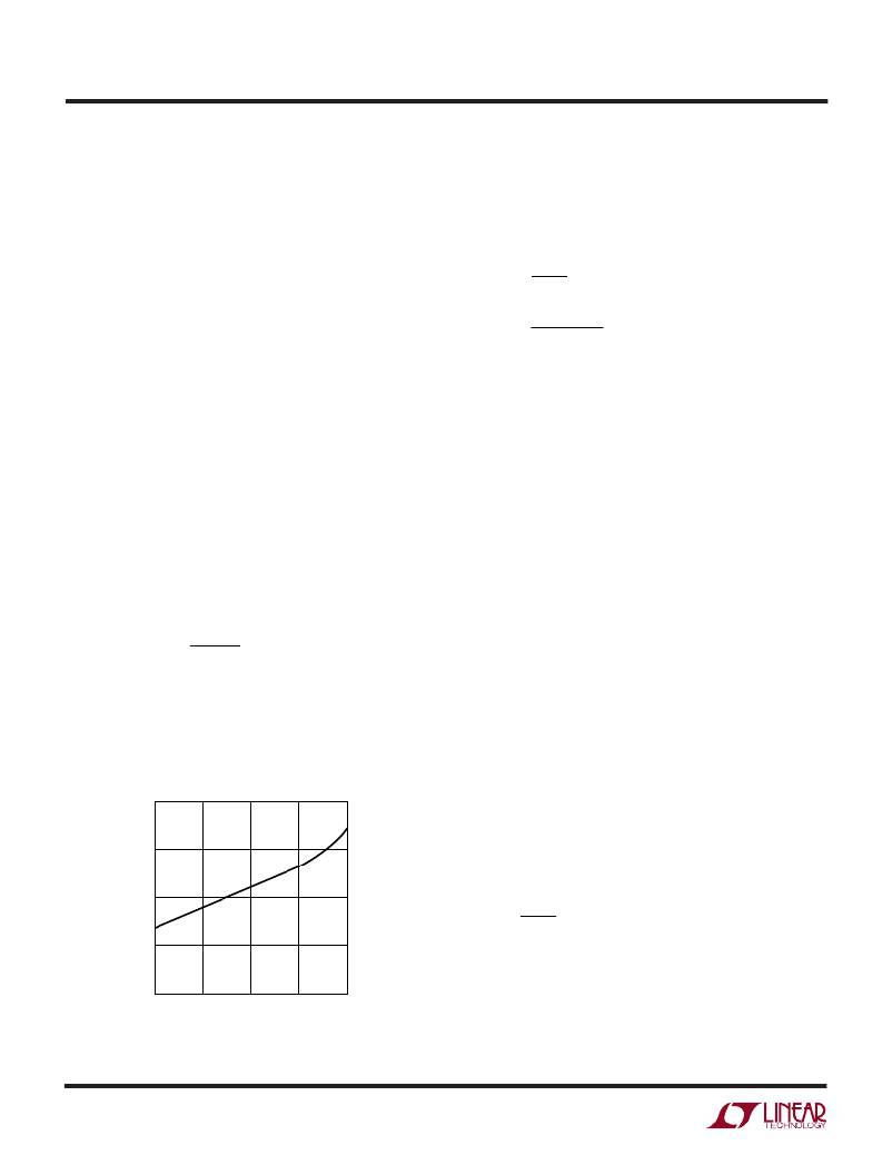
�The� ρ� T� term� is� a� normalization� factor� (unity� at� 25� °� C)�
�accounting� for� the� significant� variation� in� on-resistance�
�with� temperature,� typically� about� 0.4%/� °� C� as� shown� in�
�Figure� 2.� For� a� maximum� temperature� of� 100� °� C,� using� a�
�value� ρ� T� =� 1.3� is� reasonable.�
�2.0�
�1.5�
�The� choice� of� operating� frequency� is� a� tradeoff� between�
�efficiency� and� component� size.� Low� frequency� operation�
�improves� efficiency� by� reducing� MOSFET� switching� losses�
�but� requires� larger� inductance� and/or� capacitance� in� order�
�to� maintain� low� output� ripple� voltage.�
�The� operating� frequency� of� LTC1909-8� applications� is�
�determined� implicitly� by� the� one-shot� timer� that� controls�
�the� on-time� t� ON� of� the� top� MOSFET� switch.� The� on-time� is�
�set� by� the� current� into� the� I� ON� pin� according� to:�
�1.0�
�t� ON� =�
�V� VON�
�I� ION�
�(� 10� pF� )�
�0.5�
�Tying� a� resistor� R� ON� from� V� IN� to� the� I� ON� pin� yields� an� on-�
�0�
�–� 50�
�0�
�50�
�100�
�150�
�time� inversely� proportional� to� V� IN� .� For� a� step-down�
�converter,� this� results� in� approximately� constant� fre-�
�JUNCTION� TEMPERATURE� (� °� C)�
�quency� operation� as� the� input� supply� varies:�
�19098� F02�
�Figure� 2.� R� DS(ON)� vs.� Temperature�
�19098f�
�18�
�相关PDF资料 |
PDF描述 |
|---|---|
| H2BXG-10108-Y4-ND | JUMPER-H1501TR/A2015Y/X 8" |
| LTC1149CS-3.3#PBF | IC REG CTRLR BUCK PWM CM 16-SOIC |
| VI-JWB-EY-F2 | CONVERTER MOD DC/DC 95V 50W |
| VI-273-EW-F1 | CONVERTER MOD DC/DC 24V 100W |
| LTC3708EUH#TRPBF | IC REG CTRLR BUCK PWM CM 32-QFN |
相关代理商/技术参数 |
参数描述 |
|---|---|
| 74HC273DB | 功能描述:触发器 OCTAL D-TYPE RoHS:否 制造商:Texas Instruments 电路数量:2 逻辑系列:SN74 逻辑类型:D-Type Flip-Flop 极性:Inverting, Non-Inverting 输入类型:CMOS 输出类型: 传播延迟时间:4.4 ns 高电平输出电流:- 16 mA 低电平输出电流:16 mA 电源电压-最大:5.5 V 最大工作温度:+ 85 C 安装风格:SMD/SMT 封装 / 箱体:X2SON-8 封装:Reel |
| 74HC273DB,112 | 功能描述:触发器 OCTAL D-TYPE RoHS:否 制造商:Texas Instruments 电路数量:2 逻辑系列:SN74 逻辑类型:D-Type Flip-Flop 极性:Inverting, Non-Inverting 输入类型:CMOS 输出类型: 传播延迟时间:4.4 ns 高电平输出电流:- 16 mA 低电平输出电流:16 mA 电源电压-最大:5.5 V 最大工作温度:+ 85 C 安装风格:SMD/SMT 封装 / 箱体:X2SON-8 封装:Reel |
| 74HC273DB,118 | 功能描述:触发器 OCTAL D-TYPE RoHS:否 制造商:Texas Instruments 电路数量:2 逻辑系列:SN74 逻辑类型:D-Type Flip-Flop 极性:Inverting, Non-Inverting 输入类型:CMOS 输出类型: 传播延迟时间:4.4 ns 高电平输出电流:- 16 mA 低电平输出电流:16 mA 电源电压-最大:5.5 V 最大工作温度:+ 85 C 安装风格:SMD/SMT 封装 / 箱体:X2SON-8 封装:Reel |
| 74HC273DBT | 制造商:NXP Semiconductors 功能描述:HC/UH SERIES, POSITIVE EDGE TRIGGERED D FLIP-FLOP, TRUE OUTPUT, 20 Pin Plastic SMT |
| 74HC273DB-T | 功能描述:触发器 OCTAL D-TYPE RoHS:否 制造商:Texas Instruments 电路数量:2 逻辑系列:SN74 逻辑类型:D-Type Flip-Flop 极性:Inverting, Non-Inverting 输入类型:CMOS 输出类型: 传播延迟时间:4.4 ns 高电平输出电流:- 16 mA 低电平输出电流:16 mA 电源电压-最大:5.5 V 最大工作温度:+ 85 C 安装风格:SMD/SMT 封装 / 箱体:X2SON-8 封装:Reel |
发布紧急采购,3分钟左右您将得到回复。