- 您现在的位置:买卖IC网 > PDF目录7990 > 74LVC1G58GM,132 (NXP Semiconductors)IC CONFIG MULTI-FUNC GATE 6XSON PDF资料下载
参数资料
| 型号: | 74LVC1G58GM,132 |
| 厂商: | NXP Semiconductors |
| 文件页数: | 4/13页 |
| 文件大小: | 0K |
| 描述: | IC CONFIG MULTI-FUNC GATE 6XSON |
| 产品培训模块: | Logic Packages |
| 特色产品: | MicroPak? |
| 标准包装: | 5,000 |
| 系列: | 74LVC |
| 逻辑类型: | 可配置多功能 |
| 电路数: | 1 |
| 输入数: | 3 |
| 施密特触发器输入: | 是 |
| 输出类型: | 单端 |
| 输出电流高,低: | 32mA,32mA |
| 电源电压: | 1.65 V ~ 5.5 V |
| 工作温度: | -40°C ~ 125°C |
| 安装类型: | 表面贴装 |
| 封装/外壳: | 6-XFDFN |
| 供应商设备封装: | 6-XSON,SOT886(1.45x1) |
| 包装: | 带卷 (TR) |
| 其它名称: | 74LVC1G58GM-H 74LVC1G58GM-H-ND 935277212132 |
AR1000 SERIES RESISTIVE TOUCH SCREEN CONTROLLER
DS41393B-page 18
Preliminary
2009-2012 Microchip Technology Inc.
4.2
I2C Pin Voltage Level
Characteristics
4.3
Addressing
The AR1021’s device ID 7-bit address is: 0x4D
(0b1001101)
4.4
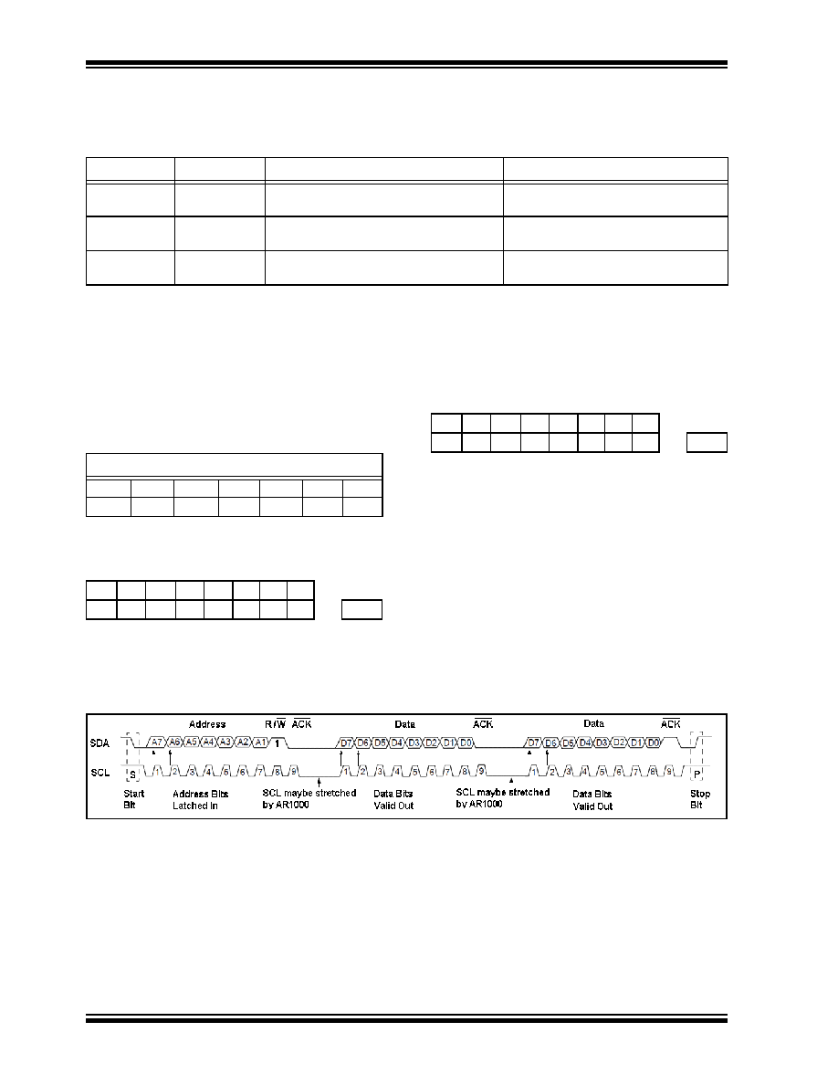
Master Read Bit Timing
Master read is to receive touch reports and command
responses from the AR1021.
Address bits are latched into the AR1021 on the
rising edges of SCL.
Data bits are latched out of the AR1021 on the
rising edges of SCL.
ACK is presented (by AR1021 for address, by
master for data) on the ninth clock.
The master must monitor the SCL pin prior to
asserting another clock pulse, as the AR1021
may be holding off the master by stretching the
clock.
FIGURE 4-1:
I2C MASTER READ BIT TIMING DIAGRAM
Steps
1.
SCL and SDA lines are Idle high.
2.
Master presents “Start” bit to the AR1021 by
taking SDA high-to-low, followed by taking SCL
high-to-low.
3.
Master presents 7-bit Address, followed by a
R/W = 1 (Read mode) bit to the AR1021 on
SDA, at the rising edge of eight master clock
(SCL) cycles.
4.
AR1021 compares the received address to its
device ID. If they match, the AR1021
acknowledges (ACK) the master sent address
by presenting a low on SDA, followed by a
low-high-low on SCL.
5.
Master monitors SCL, as the AR1021 may be
“clock stretching”, holding SCL low to indicate
that the master should wait.
TABLE 4-2:
I2C PIN VOLTAGE LEVEL CHARACTERISTICS
Function
Pin
Input
Output
SCL/SCK
SCL/SCK/TX
VSS ≤ VIL≤ 0.2*VDD
0.8*VDD ≤ VIH ≤ VDD
—
SDO
—
VSS ≤ VOL(1) ≤ (1.2V – 0.15*VDD)(2)
(1.25*VDD – 2.25V)(3) ≤ VOH(1) ≤ VDD
SDA
SDI/SDA/RX
VSS ≤ VIL ≤ 0.2*VDD
0.8*VDD ≤ VIH ≤ VDD
Open-drain
Note 1:
These parameters are characterized but not tested.
2:
At 10 mA.
3:
At –4 mA.
TABLE 4-3:
I2C DEVICE ID ADDRESS
Device ID Address, 7-bit
A7
A6
A5
A4
A3
A2
A1
10
0
1
0
1
TABLE 4-4:
I2C DEVICE WRITE ID
ADDRESS
A7
A6
A5
A4 A3 A2 A1 A0
1
0
1
010
0x9A
TABLE 4-5:
I2C DEVICE READ ID
ADDRESS
A7
A6
A5
A4 A3 A2 A1 A0
1
0
1
011
0x9B
相关PDF资料 |
PDF描述 |
|---|---|
| TXR54AB45-1810AI | ADPTR TINEL LOCK ANG SHELL 18,27 |
| 74AUP1G3208GM,132 | IC 3-IN OR-AND GATE LP 6XSON |
| TXR41AB00-1006BI | ADPTR TINEL LOCK STR SHELL 10,11 |
| TXR41AB90-1205AI | ADPTR TINEL LOCK ANG SHELL 12,13 |
| 74AUP1G3208GW,125 | IC 3-IN OR-AND GATE LP SC-88 |
相关代理商/技术参数 |
参数描述 |
|---|---|
| 74LVC1G58GM-G | 功能描述:逻辑门 3.3V LP CONFIG GATE RoHS:否 制造商:Texas Instruments 产品:OR 逻辑系列:LVC 栅极数量:2 线路数量(输入/输出):2 / 1 高电平输出电流:- 16 mA 低电平输出电流:16 mA 传播延迟时间:3.8 ns 电源电压-最大:5.5 V 电源电压-最小:1.65 V 最大工作温度:+ 125 C 安装风格:SMD/SMT 封装 / 箱体:DCU-8 封装:Reel |
| 74LVC1G58GM-H | 功能描述:逻辑门 3.3V LP CONFIG GATE RoHS:否 制造商:Texas Instruments 产品:OR 逻辑系列:LVC 栅极数量:2 线路数量(输入/输出):2 / 1 高电平输出电流:- 16 mA 低电平输出电流:16 mA 传播延迟时间:3.8 ns 电源电压-最大:5.5 V 电源电压-最小:1.65 V 最大工作温度:+ 125 C 安装风格:SMD/SMT 封装 / 箱体:DCU-8 封装:Reel |
| 74LVC1G58GN | 制造商:NXP Semiconductors 功能描述:IC CONFIG MULTI-FUNC GATE XS |
| 74LVC1G58GN,132 | 功能描述:逻辑门 Low-Power multiple function gate RoHS:否 制造商:Texas Instruments 产品:OR 逻辑系列:LVC 栅极数量:2 线路数量(输入/输出):2 / 1 高电平输出电流:- 16 mA 低电平输出电流:16 mA 传播延迟时间:3.8 ns 电源电压-最大:5.5 V 电源电压-最小:1.65 V 最大工作温度:+ 125 C 安装风格:SMD/SMT 封装 / 箱体:DCU-8 封装:Reel |
| 74LVC1G58GS,132 | 功能描述:转换 - 电压电平 18ns 5.5V 250mW RoHS:否 制造商:Micrel 类型:CML/LVDS/LVPECL to LVCMOS/LVTTL 传播延迟时间:1.9 ns 电源电流:14 mA 电源电压-最大:3.6 V 电源电压-最小:3 V 最大工作温度:+ 85 C 安装风格:SMD/SMT 封装 / 箱体:MLF-8 |
发布紧急采购,3分钟左右您将得到回复。