- 您现在的位置:买卖IC网 > PDF目录24830 > 935269556118 (NXP SEMICONDUCTORS) PLL BASED CLOCK DRIVER, 10 TRUE OUTPUT(S), 0 INVERTED OUTPUT(S), PDSO48 PDF资料下载
参数资料
| 型号: | 935269556118 |
| 厂商: | NXP SEMICONDUCTORS |
| 元件分类: | 时钟及定时 |
| 英文描述: | PLL BASED CLOCK DRIVER, 10 TRUE OUTPUT(S), 0 INVERTED OUTPUT(S), PDSO48 |
| 封装: | 6.10 MM, PLASTIC, MO-153, SOT-362-1, TSSOP-48 |
| 文件页数: | 10/12页 |
| 文件大小: | 86K |
| 代理商: | 935269556118 |
Philips Semiconductors
Product data
PCK2057
70 – 190 MHz I2C differential 1:10 clock driver
2001 Jun 12
7
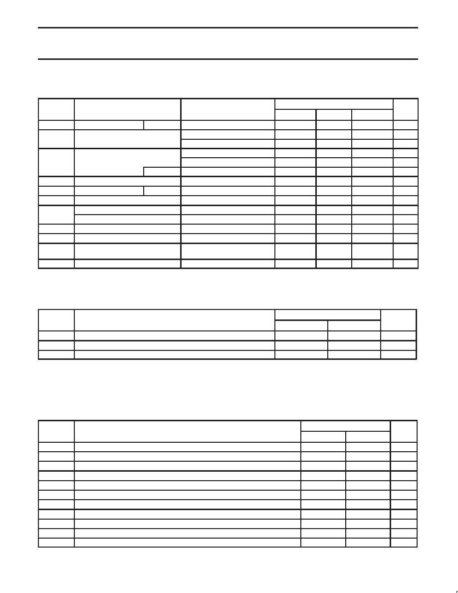
DC ELECTRICAL CHARACTERISTICS
Over recommended operating conditions.
SYMBOL
PARAMETER
TEST CONDITIONS
LIMITS
UNIT
SYMBOL
PARAMETER
TEST CONDITIONS
MIN
TYP1
MAX
UNIT
VIK
Input voltage
All inputs
VDDQ = 2.3 V; II = –18 mA
—
–1.2
V
VO
HIGH level output voltage
VDDQ = min to max; IOH = –1 mA
VDDQ – 0.1
—
V
VOH
HIGH-level output voltage
VDDQ = 2.3 V; IOH = –12 mA
1.7
—
V
LOW level output voltage
VDDQ = min to max; IOL = 1 mA
—
0.1
V
VOL
LOW-level output voltage
VDDQ = 2.3 V; IOL = 12 mA
—
0.6
V
SDA
VDDI2C = 3.0 V; IOL = 3 mA
—
0.4
V
VOX
Output differential cross voltage
VDDQ/2 – 0.2
VDDQ/2
VDDQ/2 + 0.2
V
II
Input current
CLK, FBIN
VDDQ = 2.7 V; VI = 0 V to 2.7 V
—
±10
A
IOZ
High impedance state output current
VDDQ = 2.7 V; VO = VDDQ or GND
—
±10
A
I
Power-down current on VDDQ + AVDD
CLK at 0 MHz;
Σ of IDD and AIDD
—
150
250
A
IDDPD
Power-down current on VDDI2C
CLK at 0 MHz; VDDQ = 3.6 V
—
3
20
A
IDD
Dynamic current on VDDQ
fO = 100 MHz
—
205
230
mA
AIDD
Supply current on AVDD
fO = 100 MHz
—
4
6
mA
IDDI2C
Supply current on VDDI2C
VDDI2C = 3.6 V;
SCL and SDA = 3.6V
—
1
2
mA
CI
Input capacitance
VDDQ = 2.5 V; VI = VDDQ or GND
2
2.8
3
pF
NOTES:
1. All typical values are at respective nominal VDDQ.
TIMING REQUIREMENTS
Over recommended ranges of supply voltage and operating free-air temperature.
SYMBOL
PARAMETER
LIMITS
UNIT
SYMBOL
PARAMETER
MIN
MAX
UNIT
fCLK
Clock frequency
70
190
MHz
Input clock duty cycle
40
60
%
Stabilization time 1
—
100
s
NOTE:
1. Time required for the integrated PLL circuit to obtain phase lock of its feedback signal to its reference signal. For phase lock to be obtained,
a fixed-frequency, fixed-phase reference signal must be present at CLK. Until phase lock is obtained, the specifications for propagation
delay, skew, and jitter parameters given in the switching characteristics table are not applicable. This parameter does not apply for input
modulation under SSC application.
TIMING REQUIREMENTS FOR THE I2C INTERFACE
Over recommended ranges of operating free-air temperature and VDDI2C from 3.3 V to 3.6 V..
SYMBOL
PARAMETER
STANDARD-MODE I2C-BUS
UNIT
SYMBOL
PARAMETER
MIN
MAX
UNIT
fSCL
SCL clock frequency
—
100
kHz
tBUF
Bus free time between a STOP and START condition
4.7
—
s
tSU;STA
Set-up time for a repeated START condition
4.7
—
s
tHD;STA
Hold time (repeated) START condition. After this period, the first clock is generated.
4.0
—
s
tLOW
LOW period of the SCL clock
4.7
—
s
tHIGH
HIGH period of the SCL clock
4.0
—
s
tr
Rise time of both SDA and SCL signals
—
1000
ns
tf
Fall time of both SDA and SCL signals
—
300
ns
tSU;DAT
DATA set-up time
250
—
ns
tHD;DAT
DATA hold time
0
—
ns
tSU;STO
Set-up time for STOP condition
4
—
s
相关PDF资料 |
PDF描述 |
|---|---|
| 0803-7700-05 | VDSL / PSTN CPE Splitter |
| 935269568118 | 16 I/O, PIA-GENERAL PURPOSE, PDSO24 |
| 935269651115 | 3 V FIXED POSITIVE LDO REGULATOR, 0.12 V DROPOUT, PDSO5 |
| 935269649115 | 2.5 V FIXED POSITIVE LDO REGULATOR, 0.12 V DROPOUT, PDSO5 |
| 935269652115 | 3.3 V FIXED POSITIVE LDO REGULATOR, 0.12 V DROPOUT, PDSO5 |
相关代理商/技术参数 |
参数描述 |
|---|---|
| 935269987557 | 制造商:NXP Semiconductors 功能描述:SUB ONLY TDA9587-1US1-V1.8 SUBBED TO 935269987557 |
| 935270713557 | 制造商:NXP Semiconductors 功能描述:SUB ONLY IC CHP |
| 935270792551 | 制造商:NXP Semiconductors 功能描述:IC BUFF DVR TRI-ST 16BIT 56VFBGA |
| 935270792557 | 制造商:NXP Semiconductors 功能描述:IC BUFF DVR TRI-ST 16BIT 56VFBGA |
| 935270793551 | 制造商:NXP Semiconductors 功能描述:IC BUS TRCVR 3-ST 16BIT 56VFBGA |
发布紧急采购,3分钟左右您将得到回复。