- 您现在的位置:买卖IC网 > PDF目录24830 > 935269556118 (NXP SEMICONDUCTORS) PLL BASED CLOCK DRIVER, 10 TRUE OUTPUT(S), 0 INVERTED OUTPUT(S), PDSO48 PDF资料下载
参数资料
| 型号: | 935269556118 |
| 厂商: | NXP SEMICONDUCTORS |
| 元件分类: | 时钟及定时 |
| 英文描述: | PLL BASED CLOCK DRIVER, 10 TRUE OUTPUT(S), 0 INVERTED OUTPUT(S), PDSO48 |
| 封装: | 6.10 MM, PLASTIC, MO-153, SOT-362-1, TSSOP-48 |
| 文件页数: | 5/12页 |
| 文件大小: | 86K |
| 代理商: | 935269556118 |
Philips Semiconductors
Product data
PCK2057
70 – 190 MHz I2C differential 1:10 clock driver
2
2001 Jun 12
853–2253 26485
FEATURES
Optimized for clock distribution in DDR (Double Data Rate)
SDRAM applications supporting DDR 200/266/300/333
Full DDR solution provided when used with PCK2002P or
PCK2002PL, and PCK2022RA
1-to-10 differential clock distribution
Very low jitter (< 100 ps)
Operation from 2.2 V to 2.7 V AV
DD and 2.3 V to 2.7 V VDD
SSTL_2 interface clock inputs and outputs
HCSL to SSTL_2 input conversion
Test mode enables buffers while disabling PLL
Tolerant of Spread Spectrum input clock
3.3 V I2C support with 3.3 V V
DDI
2C
2.5 V I2C support with 2.5 V V
DDI
2C
Form, fit, and function compatible with CDCV850
DESCRIPTION
The PCK2057 is a high-performance, low-skew, low-jitter zero delay
buffer that distributes a differential clock input pair (CLK, CLK) to ten
differential pairs of clock outputs and one differential pair of
feedback clock outputs. The clock outputs are controlled by the
clock inputs (CLK, CLK), the feedback clocks (FBIN, FBIN), the
2-line serial interface (SDA, SCL), and the analog power input
(AVDD). The two-line serial interface (I2C) can put the individual
output clock pairs in a high-impedance state. When AVDD is tied to
GND, the PLL is turned off and bypassed for test purposes.
The device provides a standard mode (100 kbits) I2C interface for
device control. The implementation is as a slave/receiver. The serial
inputs (SDA, SCL) provide integrated pull-up resistors (typically
100 k
).
Two 8-bit, 2-line serial registers provide individual enable control for
each output pair. All outputs default to enabled at power-up. Each
output pair can be placed in a high-impedance mode, when a
low-level control bit is written to the control register. The registers
must be accessed in sequential order (i.e., random access of the
registers is not supported). The I2C interface circuit can be supplied
with either 2.5 V or 3.3 V (VDDI2C).
Since the PCK2057 is based on PLL circuitry, it requires a
stabilization time to achieve phase-lock of the PLL. This stabilization
time is required following power-up.
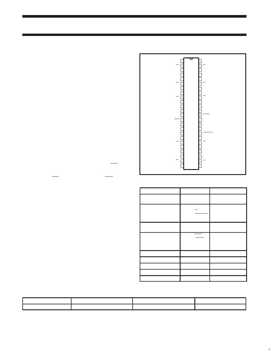
PIN CONFIGURATION
1
2
3
4
5
6
7
8
9
10
11
12
13
14
15
16
17
18
19
20
25
26
27
28
29
30
31
32
33
34
35
36
37
38
39
40
21
22
23
24
41
42
43
44
45
46
47
48
GND
Y0
VDDQ
Y1
GND
Y2
GND
Y2
VDDQ
SCL
CLK
VDDI2C
AVDD
AGND
GND
Y3
VDDQ
Y4
GND
Y5
VDDQ
Y6
GND
Y7
VDDQ
SDA
FBIN
VDDQ
FBOUT
GND
Y8
VDDQ
Y9
SW00506
GND
PIN DESCRIPTION
PINS
SYMBOL
DESCRIPTION
1, 7, 8, 18, 24, 25, 31,
41, 42, 48
GND
Ground
2, 3, 5, 6, 9, 10, 19, 20,
22, 23, 26, 27, 29, 30,
32, 33, 39, 40, 43, 44,
46, 47
Yn, Yn,
FBOUT, FBOUT
Buffered output
copies of input clock,
CLK
4, 11, 21, 28, 34, 38,
45
VDDQ
2.5 V supply
13, 14, 35, 36
CLK, CLK,
FBIN, FBIN
Differential clock
inputs and feedback
differential clock
inputs
16
AVDD
Analog power
17
AGND
Analog ground
37
SDA
Serial data
12
SCL
Serial clock
15
VDDI2C
I2C power
ORDERING INFORMATION
PACKAGES
TEMPERATURE RANGE
ORDER CODE
DRAWING NUMBER
48-Pin Plastic TSSOP
0 to +70
°C
PCK2057DGG
SOT362-1
相关PDF资料 |
PDF描述 |
|---|---|
| 0803-7700-05 | VDSL / PSTN CPE Splitter |
| 935269568118 | 16 I/O, PIA-GENERAL PURPOSE, PDSO24 |
| 935269651115 | 3 V FIXED POSITIVE LDO REGULATOR, 0.12 V DROPOUT, PDSO5 |
| 935269649115 | 2.5 V FIXED POSITIVE LDO REGULATOR, 0.12 V DROPOUT, PDSO5 |
| 935269652115 | 3.3 V FIXED POSITIVE LDO REGULATOR, 0.12 V DROPOUT, PDSO5 |
相关代理商/技术参数 |
参数描述 |
|---|---|
| 935269987557 | 制造商:NXP Semiconductors 功能描述:SUB ONLY TDA9587-1US1-V1.8 SUBBED TO 935269987557 |
| 935270713557 | 制造商:NXP Semiconductors 功能描述:SUB ONLY IC CHP |
| 935270792551 | 制造商:NXP Semiconductors 功能描述:IC BUFF DVR TRI-ST 16BIT 56VFBGA |
| 935270792557 | 制造商:NXP Semiconductors 功能描述:IC BUFF DVR TRI-ST 16BIT 56VFBGA |
| 935270793551 | 制造商:NXP Semiconductors 功能描述:IC BUS TRCVR 3-ST 16BIT 56VFBGA |
发布紧急采购,3分钟左右您将得到回复。