参数资料
| 型号: | A3PE3000-1FG324 |
| 厂商: | Microsemi SoC |
| 文件页数: | 143/162页 |
| 文件大小: | 0K |
| 描述: | IC FPGA 1KB FLASH 3M 324-FBGA |
| 标准包装: | 84 |
| 系列: | ProASIC3E |
| RAM 位总计: | 516096 |
| 输入/输出数: | 221 |
| 门数: | 3000000 |
| 电源电压: | 1.425 V ~ 1.575 V |
| 安装类型: | 表面贴装 |
| 工作温度: | 0°C ~ 70°C |
| 封装/外壳: | 324-BGA |
| 供应商设备封装: | 324-FBGA(19x19) |
第1页第2页第3页第4页第5页第6页第7页第8页第9页第10页第11页第12页第13页第14页第15页第16页第17页第18页第19页第20页第21页第22页第23页第24页第25页第26页第27页第28页第29页第30页第31页第32页第33页第34页第35页第36页第37页第38页第39页第40页第41页第42页第43页第44页第45页第46页第47页第48页第49页第50页第51页第52页第53页第54页第55页第56页第57页第58页第59页第60页第61页第62页第63页第64页第65页第66页第67页第68页第69页第70页第71页第72页第73页第74页第75页第76页第77页第78页第79页第80页第81页第82页第83页第84页第85页第86页第87页第88页第89页第90页第91页第92页第93页第94页第95页第96页第97页第98页第99页第100页第101页第102页第103页第104页第105页第106页第107页第108页第109页第110页第111页第112页第113页第114页第115页第116页第117页第118页第119页第120页第121页第122页第123页第124页第125页第126页第127页第128页第129页第130页第131页第132页第133页第134页第135页第136页第137页第138页第139页第140页第141页第142页当前第143页第144页第145页第146页第147页第148页第149页第150页第151页第152页第153页第154页第155页第156页第157页第158页第159页第160页第161页第162页
ProASIC3E Flash Family FPGAs
Revision 13
2-67
Global Resource Characteristics
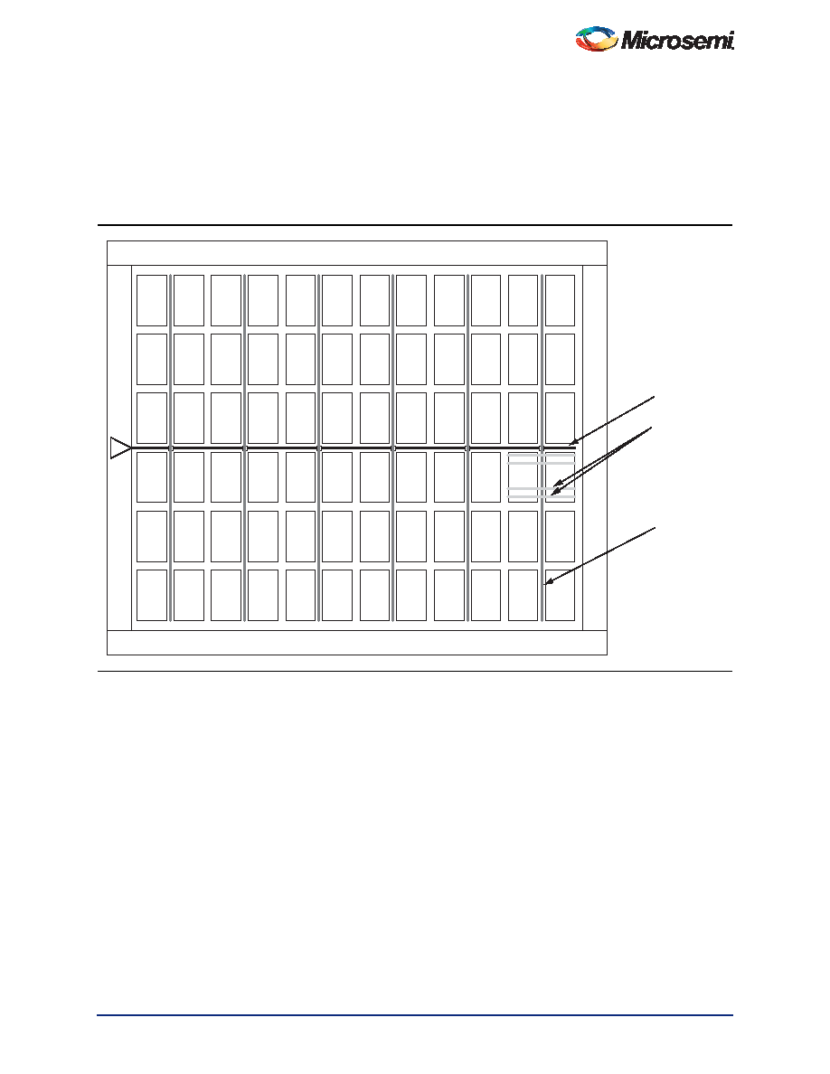
A3PE600 Clock Tree Topology
Clock delays are device-specific. Figure 2-38 is an example of a global tree used for clock routing. The
global tree presented in Figure 2-38 is driven by a CCC located on the west side of the A3PE600 device.
It is used to drive all D-flip-flops in the device.
Global Tree Timing Characteristics
Global clock delays include the central rib delay, the spine delay, and the row delay. Delays do not
include I/O input buffer clock delays, as these are I/O standard–dependent, and the clock may be driven
and conditioned internally by the CCC module. For more details on clock conditioning capabilities, refer
page 2-68, and Table 2-97 on page 2-68 present minimum and maximum global clock delays within the
device. Minimum and maximum delays are measured with minimum and maximum loading.
Figure 2-38 Example of Global Tree Use in an A3PE600 Device for Clock Routing
Central
Global Rib
VersaTile
Rows
Global Spine
CCC
相关PDF资料 |
PDF描述 |
|---|---|
| A3PE3000L-FGG324 | IC FPGA 1KB FLASH 3M 324-FBGA |
| A3PE3000-1FGG324 | IC FPGA 1KB FLASH 3M 324-FBGA |
| A3PE3000L-FG324 | IC FPGA 1KB FLASH 3M 324-FBGA |
| M1A3PE3000-1FG324 | IC FPGA 1KB FLASH 3M 324-FBGA |
| M1A3PE3000-1FGG324 | IC FPGA 1KB FLASH 3M 324-FBGA |
相关代理商/技术参数 |
参数描述 |
|---|---|
| A3PE3000-1FG324I | 功能描述:IC FPGA 1KB FLASH 3M 324-FBGA RoHS:否 类别:集成电路 (IC) >> 嵌入式 - FPGA(现场可编程门阵列) 系列:ProASIC3E 标准包装:1 系列:ProASICPLUS LAB/CLB数:- 逻辑元件/单元数:- RAM 位总计:129024 输入/输出数:248 门数:600000 电源电压:2.3 V ~ 2.7 V 安装类型:表面贴装 工作温度:- 封装/外壳:352-BFCQFP,带拉杆 供应商设备封装:352-CQFP(75x75) |
| A3PE3000-1FG484 | 功能描述:IC FPGA 1KB FLASH 3M 484-FBGA RoHS:否 类别:集成电路 (IC) >> 嵌入式 - FPGA(现场可编程门阵列) 系列:ProASIC3E 产品培训模块:Three Reasons to Use FPGA's in Industrial Designs Cyclone IV FPGA Family Overview 特色产品:Cyclone? IV FPGAs 标准包装:60 系列:CYCLONE® IV GX LAB/CLB数:9360 逻辑元件/单元数:149760 RAM 位总计:6635520 输入/输出数:270 门数:- 电源电压:1.16 V ~ 1.24 V 安装类型:表面贴装 工作温度:0°C ~ 85°C 封装/外壳:484-BGA 供应商设备封装:484-FBGA(23x23) |
| A3PE3000-1FG484I | 功能描述:IC FPGA 1KB FLASH 3M 484-FBGA RoHS:否 类别:集成电路 (IC) >> 嵌入式 - FPGA(现场可编程门阵列) 系列:ProASIC3E 标准包装:1 系列:ProASICPLUS LAB/CLB数:- 逻辑元件/单元数:- RAM 位总计:129024 输入/输出数:248 门数:600000 电源电压:2.3 V ~ 2.7 V 安装类型:表面贴装 工作温度:- 封装/外壳:352-BFCQFP,带拉杆 供应商设备封装:352-CQFP(75x75) |
| A3PE3000-1FG896 | 功能描述:IC FPGA 1KB FLASH 3M 896-FBGA RoHS:否 类别:集成电路 (IC) >> 嵌入式 - FPGA(现场可编程门阵列) 系列:ProASIC3E 产品培训模块:Three Reasons to Use FPGA's in Industrial Designs Cyclone IV FPGA Family Overview 特色产品:Cyclone? IV FPGAs 标准包装:60 系列:CYCLONE® IV GX LAB/CLB数:9360 逻辑元件/单元数:149760 RAM 位总计:6635520 输入/输出数:270 门数:- 电源电压:1.16 V ~ 1.24 V 安装类型:表面贴装 工作温度:0°C ~ 85°C 封装/外壳:484-BGA 供应商设备封装:484-FBGA(23x23) |
| A3PE3000-1FG896ES | 制造商:ACTEL 制造商全称:Actel Corporation 功能描述:ProASIC3E Flash Family FPGAs |
发布紧急采购,3分钟左右您将得到回复。