参数资料
| 型号: | A40MX04-2PLG84 |
| 厂商: | Microsemi SoC |
| 文件页数: | 121/142页 |
| 文件大小: | 0K |
| 描述: | IC FPGA MX SGL CHIP 6K 84-PLCC |
| 标准包装: | 16 |
| 系列: | MX |
| 输入/输出数: | 69 |
| 门数: | 6000 |
| 电源电压: | 3 V ~ 3.6 V,4.75 V ~ 5.25 V |
| 安装类型: | 表面贴装 |
| 工作温度: | 0°C ~ 70°C |
| 封装/外壳: | 84-LCC(J 形引线) |
| 供应商设备封装: | 84-PLCC(29.31x29.31) |
第1页第2页第3页第4页第5页第6页第7页第8页第9页第10页第11页第12页第13页第14页第15页第16页第17页第18页第19页第20页第21页第22页第23页第24页第25页第26页第27页第28页第29页第30页第31页第32页第33页第34页第35页第36页第37页第38页第39页第40页第41页第42页第43页第44页第45页第46页第47页第48页第49页第50页第51页第52页第53页第54页第55页第56页第57页第58页第59页第60页第61页第62页第63页第64页第65页第66页第67页第68页第69页第70页第71页第72页第73页第74页第75页第76页第77页第78页第79页第80页第81页第82页第83页第84页第85页第86页第87页第88页第89页第90页第91页第92页第93页第94页第95页第96页第97页第98页第99页第100页第101页第102页第103页第104页第105页第106页第107页第108页第109页第110页第111页第112页第113页第114页第115页第116页第117页第118页第119页第120页当前第121页第122页第123页第124页第125页第126页第127页第128页第129页第130页第131页第132页第133页第134页第135页第136页第137页第138页第139页第140页第141页第142页
40MX and 42MX FPGA Families
1- 4
R ev isio n 1 1
provides capability to quickly design memory functions with the SRAM blocks. Unused SRAM blocks can
be used to implement registers for other user logic within the design.
Routing Structure
The MX architecture uses vertical and horizontal routing tracks to interconnect the various logic and I/O
modules. These routing tracks are metal interconnects that may be continuous or split into segments.
Varying segment lengths allow the interconnect of over 90% of design tracks to occur with only two
antifuse connections. Segments can be joined together at the ends using antifuses to increase their
lengths up to the full length of the track. All interconnects can be accomplished with a maximum of four
antifuses.
Horizontal Routing
Horizontal routing tracks span the whole row length or are divided into multiple segments and are located
in between the rows of modules. Any segment that spans more than one-third of the row length is
considered a long horizontal segment. A typical channel is shown in Figure 1-6. Within horizontal routing,
dedicated routing tracks are used for global clock networks and for power and ground tie-off tracks. Non-
dedicated tracks are used for signal nets.
Vertical Routing
Another set of routing tracks run vertically through the module. There are three types of vertical tracks:
input, output, and long. Long tracks span the column length of the module, and can be divided into
multiple segments. Each segment in an input track is dedicated to the input of a particular module; each
segment in an output track is dedicated to the output of a particular module. Long segments are
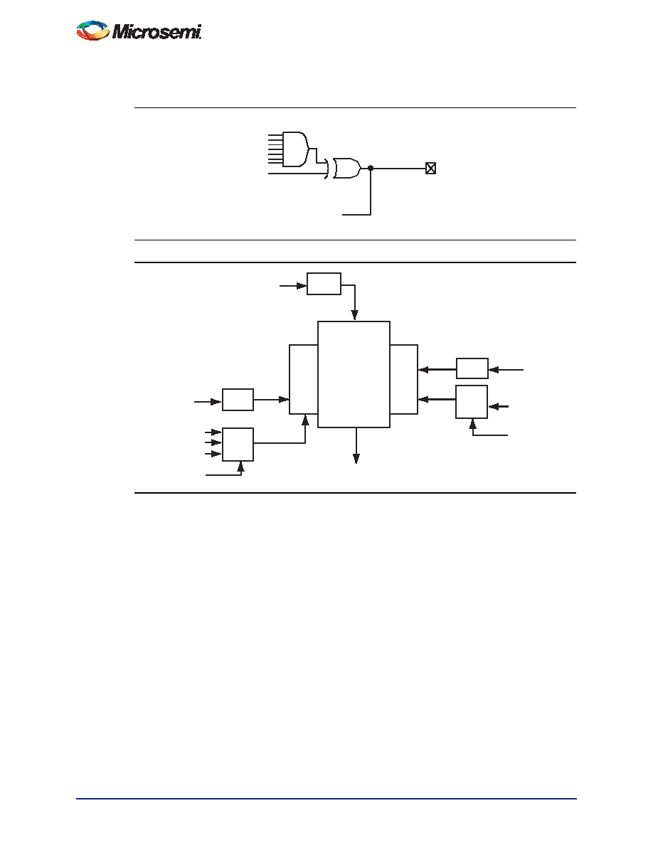
Figure 1-4
A42MX24 and A42MX36 D-Module Implementation
Figure 1-5
A42MX36 Dual-Port SRAM Block
7 Inputs
Hard-Wire to I/O
Feedback to Array
Programmable
Inverter
SRAM Module
32 x 8 or 64 x 4
(256 Bits)
Read
Port
Logic
Write
Port
Logic
RD[7:0]
Routing Tracks
Latches
Read
Logic
[5:0]
RDAD[5:0]
REN
RCLK
Latches
WD[7:0]
Latches
WRAD[5:0]
Write
Logic
MODE
BLKEN
WEN
WCLK
[5:0]
[7:0]
相关PDF资料 |
PDF描述 |
|---|---|
| IDT71024S15YGI8 | IC SRAM 1MBIT 15NS 32SOJ |
| A40MX04-2PL84 | IC FPGA MX SGL CHIP 6K 84-PLCC |
| APA150-FGG144 | IC FPGA PROASIC+ 150K 144-FBGA |
| APA150-FG144 | IC FPGA PROASIC+ 150K 144-FBGA |
| AMM25DRSD-S288 | CONN EDGECARD 50POS .156 EXTEND |
相关代理商/技术参数 |
参数描述 |
|---|---|
| A40MX04-2PLG84I | 功能描述:IC FPGA MX SGL CHIP 6K 84-PLCC RoHS:是 类别:集成电路 (IC) >> 嵌入式 - FPGA(现场可编程门阵列) 系列:MX 标准包装:90 系列:ProASIC3 LAB/CLB数:- 逻辑元件/单元数:- RAM 位总计:36864 输入/输出数:157 门数:250000 电源电压:1.425 V ~ 1.575 V 安装类型:表面贴装 工作温度:-40°C ~ 125°C 封装/外壳:256-LBGA 供应商设备封装:256-FPBGA(17x17) |
| A40MX04-2PQ100 | 功能描述:IC FPGA MX SGL CHIP 6K 100-PQFP RoHS:否 类别:集成电路 (IC) >> 嵌入式 - FPGA(现场可编程门阵列) 系列:MX 标准包装:90 系列:ProASIC3 LAB/CLB数:- 逻辑元件/单元数:- RAM 位总计:36864 输入/输出数:157 门数:250000 电源电压:1.425 V ~ 1.575 V 安装类型:表面贴装 工作温度:-40°C ~ 125°C 封装/外壳:256-LBGA 供应商设备封装:256-FPBGA(17x17) |
| A40MX04-2PQ100I | 功能描述:IC FPGA MX SGL CHIP 6K 100-PQFP RoHS:否 类别:集成电路 (IC) >> 嵌入式 - FPGA(现场可编程门阵列) 系列:MX 标准包装:90 系列:ProASIC3 LAB/CLB数:- 逻辑元件/单元数:- RAM 位总计:36864 输入/输出数:157 门数:250000 电源电压:1.425 V ~ 1.575 V 安装类型:表面贴装 工作温度:-40°C ~ 125°C 封装/外壳:256-LBGA 供应商设备封装:256-FPBGA(17x17) |
| A40MX04-2PQ100M | 制造商:未知厂家 制造商全称:未知厂家 功能描述:Field Programmable Gate Array (FPGA) |
| A40MX04-2PQG100 | 功能描述:IC FPGA MX SGL CHIP 6K 100-PQFP RoHS:是 类别:集成电路 (IC) >> 嵌入式 - FPGA(现场可编程门阵列) 系列:MX 标准包装:90 系列:ProASIC3 LAB/CLB数:- 逻辑元件/单元数:- RAM 位总计:36864 输入/输出数:157 门数:250000 电源电压:1.425 V ~ 1.575 V 安装类型:表面贴装 工作温度:-40°C ~ 125°C 封装/外壳:256-LBGA 供应商设备封装:256-FPBGA(17x17) |
发布紧急采购,3分钟左右您将得到回复。