- 您现在的位置:买卖IC网 > PDF目录294789 > A42MX36-CQ208A FPGA, 54000 GATES, CQFP208 PDF资料下载
参数资料
| 型号: | A42MX36-CQ208A |
| 元件分类: | FPGA |
| 英文描述: | FPGA, 54000 GATES, CQFP208 |
| 封装: | CERAMIC, QFP-208 |
| 文件页数: | 3/76页 |
| 文件大小: | 429K |
| 代理商: | A42MX36-CQ208A |
第1页第2页当前第3页第4页第5页第6页第7页第8页第9页第10页第11页第12页第13页第14页第15页第16页第17页第18页第19页第20页第21页第22页第23页第24页第25页第26页第27页第28页第29页第30页第31页第32页第33页第34页第35页第36页第37页第38页第39页第40页第41页第42页第43页第44页第45页第46页第47页第48页第49页第50页第51页第52页第53页第54页第55页第56页第57页第58页第59页第60页第61页第62页第63页第64页第65页第66页第67页第68页第69页第70页第71页第72页第73页第74页第75页第76页
MX Automotive Family FPGAs
v2.0
1-5
Antifuse Structures
An antifuse is a “normally open” structure as opposed to
the normally connected fuse structure used in PROMs or
PALs. The use of antifuses to implement a programmable
logic device results in highly testable structures as well as
efficient programming algorithms. The structure is
highly-testable
because
there
are
no
pre-existing
connections; therefore, temporary connections can be
made
using
pass
transistors.
These
temporary
connections can isolate individual antifuses to be
programmed and individual circuit structures to be
tested,
which
can
be
done
before
and
after
programming. For example, all metal tracks can be
tested for continuity and shorts between adjacent tracks,
and the functionality of all logic modules can be verified.
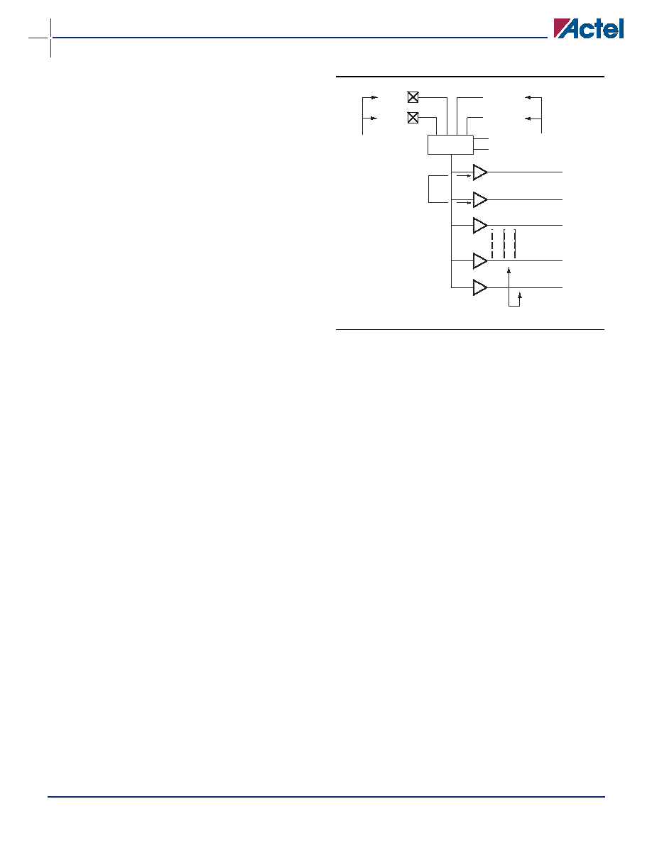
Clock Networks
The 40MX devices have one global clock distribution
network
(CLK).
Two
low-skew,
high-fanout
clock
distribution networks are provided in each 42MX device.
These networks are referred to as CLK0 and CLK1. Each
network has a clock module (CLKMOD) that selects the
source of the clock signal and may be driven as follows:
Externally from the CLKA pad
Externally from the CLKB pad
Internally from the CLKINTA input
Internally from the CLKINTB input
The clock modules are located in the top row of I/O
modules. Clock drivers and a dedicated horizontal clock
track are located in each horizontal routing channel.
The user controls the clock module by selecting one of
two clock macros from the macro library. The macro
CLKBUF is used to connect one of the two external clock
pins to a clock network, and the macro CLKINT is used to
connect an internally-generated clock signal to a clock
network. Since both clock networks are identical, it does
not matter whether CLK0 or CLK1 is being used. The
clock input pads can also be used as normal I/Os,
bypassing the clock networks (Figure 1-8).
The A42MX36 device has four additional register control
resources, called quadrant clock networks (Figure 1-9 on
page 1-6). Each quadrant clock provides a local, high-
fanout resource to the contiguous logic modules within
its quadrant of the device. Quadrant clock signals can
originate from specific I/O pins or from the internal array
and can be used as a secondary register clock, register
clear, or output enable.
Test Circuitry
All MX automotive-grade
devices contain
probing
circuitry which test and debug a design once it is
programmed into a device. The test circuitry allows the
designer to probe any internal node during device
operation to aid in debugging a design.
IEEE Standard 1149.1 Boundary
Scan Testing (BST)
A42MX24 and A42MX36 devices contain IEEE Standard
1149.1 boundary scan test circuitry. IEEE Standard 1149.1
defines a four-pin Test Access Port (TAP) interface for
testing integrated circuits in a system. The A42MX24 and
A42MX36 devices provide the following BST pins: Test
Data In (TDI), Test Data Out (TDO), Test Clock (TCK), and
Test Mode Select (TMS). Devices are configured in a test
“chain” where BST data can be transmitted serially
between devices via TDO-to-TDI interconnections. The
TMS and TCK signals are shared among all devices in the
test chain so that all components operate in the same
state.
The 42MX family implements a subset of the IEEE
Standard 1149.1 BST instruction in addition to a private
instruction.
Refer
to
the
IEEE
Standard
1149.1
specification for detailed information regarding BST.
Boundary Scan Circuitry
The A42MX24 and A42MX36 boundary-scan circuitry
consists of a Test Access Port (TAP) controller, test
instruction register, a bypass register, and a boundary
scan register. Figure 1-10 on page 1-6 shows a block
diagram of the 42MX boundary scan circuitry.
Figure 1-8 42MX Clock Networks
CLKB
CLKA
From
Pads
Clock
Drivers
CLKMOD
CLKINB
CLKINA
S0
S1
Internal
Signal
CLKO(17)
CLKO(16)
CLKO(15)
CLKO(2)
CLKO(1)
Clock Tracks
相关PDF资料 |
PDF描述 |
|---|---|
| A42MX36-CQ256A | FPGA, 54000 GATES, CQFP256 |
| A42MX36-1RQ208I | FPGA, 2438 CLBS, 36000 GATES, 91 MHz, PQFP208 |
| A42MX36-1RQ208 | FPGA, 2438 CLBS, 36000 GATES, 91 MHz, PQFP208 |
| A42MX36-1RQG208I | FPGA, 2438 CLBS, 36000 GATES, 91 MHz, PQFP208 |
| A42MX36-1RQG208 | FPGA, 2438 CLBS, 36000 GATES, 91 MHz, PQFP208 |
相关代理商/技术参数 |
参数描述 |
|---|---|
| A42MX36-CQ208B | 功能描述:IC FPGA MX SGL CHIP 54K 208-CQFP RoHS:否 类别:集成电路 (IC) >> 嵌入式 - FPGA(现场可编程门阵列) 系列:MX 标准包装:1 系列:ProASICPLUS LAB/CLB数:- 逻辑元件/单元数:- RAM 位总计:129024 输入/输出数:248 门数:600000 电源电压:2.3 V ~ 2.7 V 安装类型:表面贴装 工作温度:- 封装/外壳:352-BFCQFP,带拉杆 供应商设备封装:352-CQFP(75x75) |
| A42MX36-CQ208M | 制造商:Microsemi Corporation 功能描述:FPGA 54K GATES 1184 CELLS 79MHZ/131MHZ 0.45UM 3.3V/5V 208CQF - Trays 制造商:Microsemi Corporation 功能描述:IC FPGA 176 I/O 208CQFP 制造商:Microsemi Corporation 功能描述:IC FPGA MX SGL CHIP 54K 208-CQFP |
| A42MX36-CQ256 | 功能描述:IC FPGA MX SGL CHIP 54K 256-CQFP RoHS:否 类别:集成电路 (IC) >> 嵌入式 - FPGA(现场可编程门阵列) 系列:MX 标准包装:1 系列:ProASICPLUS LAB/CLB数:- 逻辑元件/单元数:- RAM 位总计:129024 输入/输出数:248 门数:600000 电源电压:2.3 V ~ 2.7 V 安装类型:表面贴装 工作温度:- 封装/外壳:352-BFCQFP,带拉杆 供应商设备封装:352-CQFP(75x75) |
| A42MX36-CQ256B | 功能描述:IC FPGA MX SGL CHIP 54K 256-CQFP RoHS:否 类别:集成电路 (IC) >> 嵌入式 - FPGA(现场可编程门阵列) 系列:MX 标准包装:1 系列:ProASICPLUS LAB/CLB数:- 逻辑元件/单元数:- RAM 位总计:129024 输入/输出数:248 门数:600000 电源电压:2.3 V ~ 2.7 V 安装类型:表面贴装 工作温度:- 封装/外壳:352-BFCQFP,带拉杆 供应商设备封装:352-CQFP(75x75) |
| A42MX36-CQ256M | 制造商:Microsemi Corporation 功能描述:FPGA 54K GATES 1184 CELLS 79MHZ/131MHZ 0.45UM 3.3V/5V 256CQF - Trays 制造商:Microsemi Corporation 功能描述:IC FPGA 202 I/O 256CQFP |
发布紧急采购,3分钟左右您将得到回复。