参数资料
| 型号: | A4447SLJTR-T |
| 厂商: | Allegro Microsystems Inc |
| 文件页数: | 9/12页 |
| 文件大小: | 0K |
| 描述: | IC REG BUCK ADJ 2A 8SOIC |
| 标准包装: | 1 |
| 类型: | 降压(降压) |
| 输出类型: | 可调式 |
| 输出数: | 1 |
| 输出电压: | 0.8 V ~ 24 V |
| 输入电压: | 8 V ~ 50 V |
| PWM 型: | 电流模式 |
| 电流 - 输出: | 2A |
| 同步整流器: | 无 |
| 工作温度: | -20°C ~ 85°C |
| 安装类型: | 表面贴装 |
| 封装/外壳: | 8-SOIC(0.154",3.90mm Width)裸露焊盘 |
| 包装: | 标准包装 |
| 供应商设备封装: | 8-SOIC-EP |
| 产品目录页面: | 1141 (CN2011-ZH PDF) |
| 其它名称: | 620-1329-6 |
�� �
�
�A4447�
�High� Voltage� Step� Down� Regulator�
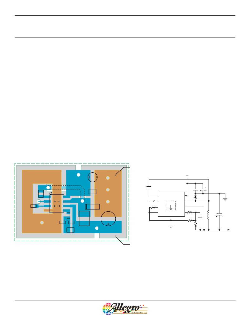
�Recommended� PCB� Layout�
�In� order� to� minimize� the� effects� of� ground� bounce� and� offset�
�issues,� it� is� important� to� have� a� low� impedance� ground� located�
�very� close� to� the� device.� This� grounding� scheme� is� known� as� star�
�grounding.� It� is� likely� that� a� ground� plane� will� be� necessary� to�
�meet� thermal� requirements.� The� recommended� land� pattern� illus-�
�trates� how� to� create� a� low� impedance� ground� that� will� also� assist�
�with� removing� thermal� energy� from� the� device.�
�The� input� capacitor� must� be� placed� as� close� as� possible� to� the�
�VIN� terminal� because� during� the� on� cycle� it� is� responsible� for�
�supplying� the� current� to� the� switcher.� During� the� off� cycle,� the�
�current� path� is� from� the� negative� terminal� of� the� COUT� cap,�
�through� the� diode� and� inductor,� and� then� to� the� load.� As� a� result,�
�COUT� and� the� rectifier� diode� must� share� the� connection� at� the�
�negative� terminal� of� the� CIN� capacitor� in� order� to� reduce� ground�
�bounce� when� the� diode� is� conducting.�
�CIN1�
�VIN�
�GND�
�The� inductor� should� be� connected� as� close� as� possible� to� the�
�switching� node� to� minimize� noise.� Some� applications� may� require�
�a� shielded� inductor� due� to� EMI� restrictions.� This� will� depend� on�
�the� application� and� parameters� defined� by� the� system� that� will�
�host� the� regulator.�
�The� high� voltage-switching� node� could� affect� R� TSET� .� If� longer�
�off-times� are� used,� the� resistance� on� the� RTSET� pin� can� be� quite�
�large.� When� designing� the� layout,� try� to� keep� RTSET� away� from�
�the� inductor� and� switching� node.� It� is� also� beneficial� to� keep� the�
�trace� as� short� as� possible� to� reduce� the� effect� of� noise� injection.�
�Because� of� this� layout� guideline,� the� TSET� pin� is� located� on� the�
�other� side� of� the� device,� away� from� the� switching� node.�
�The� FB� resistor� network� should� have� a� lower� impedance� to� avoid�
�interference� from� the� switching� node.� Because� the� impedance�
�on� the� FB� node� can� be� controlled,� it� is� not� as� critical� to� keep� the�
�network� isolated.� It� is� important� to� keep� the� ground� trace� short� so�
�that� ground� bounce� cannot� effect� the� output� voltage� regulation.�
�Star� Ground�
�V� IN�
�CIN2�
�CBOOT�
�CIN2�
�CIN1�
�CBOOT�
�RTSET�
�U1�
�R3�
�D1�
�GND�
�GND�
�1�
�RTSET�
�BOOT�
�ENB�
�TSET�
�GND�
�A4447�
�PAD�
�VIN�
�LX�
�VBIAS�
�FB�
�R3�
�R2�
�D1�
�C� BYP�
�L1�
�COUT�
�GND�
�R2�
�R1�
�L1�
�COUT�
�R1�
�V� OUT�
�CBYP�
�VOUT�
�Exposed� copper� thermal�
�ground� area� on� the�
�unpopulated� side� of� the� PCB�
�The� large� star� ground� area� on� the� populated� side� of� the� PCB,� shown� in� the� diagram� as� the� GND� nodes,� supports� high� current� throughput,� and� allows�
�the� VOUT� node� to� be� located� as� close� as� practical� to� the� A4447� (U1).� Thermal� conduction� from� the� A4447� is� enhanced� by� direct� contact� of� its�
�exposed� thermal� pad� to� the� smaller� ground� area� under� the� A4447.� This� area� is� connected� by� thermal� vias� to� the� large� copper� ground� plane� on� the�
�unpopulated� side� of� the� PCB.�
�Allegro� MicroSystems,� LLC�
�115� Northeast� Cutoff�
�Worcester,� Massachusetts� 01615-0036� U.S.A.�
�1.508.853.5000;� www.allegromicro.com�
�9�
�相关PDF资料 |
PDF描述 |
|---|---|
| A4490EES-T | IC REG BUCK ADJ 1.5A TRPL 20QFN |
| A4491EESTR-T | IC REG BUCK ADJ 2.2A TRPL 20QFN |
| A4931MET-T | IC DC MOTOR PREDRIVER 3PH 28QFN |
| A4934GLPTR-T | IC BLDC DVR 3PHASE 16-ETSSOP |
| A4936METTR-T | IC DC MOTOR PREDRIVER 3PH 32QFN |
相关代理商/技术参数 |
参数描述 |
|---|---|
| A4448RT | 制造商:Pentair Technical Products / Hoffman 功能描述:Wiring Trough 4.00x4.00x48.00 , 4.00x4.00x48.00, Steel |
| A-4448RT | 制造商:Pentair Technical Products / Hoffman 功能描述:Wiring Trough 4.00x4.00x48.00 |
| A4448T1T | 制造商:Pentair Technical Products / Hoffman 功能描述:4X4, 48 LONG TYPE 1 TROUGH Gray, 4.00x4.00x48.00, Steel |
| A445 | 制造商:未知厂家 制造商全称:未知厂家 功能描述:DISPLAY 0-20 OR 24MA |
| A4450KESTR-J | 功能描述:Buck-Boost Regulator Positive Output Step-Up/Step-Down DC-DC Controller IC 20-QFN (4x4) 制造商:allegro microsystems, llc 系列:汽车级,AEC-Q100 包装:剪切带(CT) 零件状态:新产品 输出类型:晶体管驱动器 功能:升压/降压 输出配置:正 拓扑:降压-升压 输出数:1 输出阶段:1 电压 - 电源(Vcc/Vdd):3 V ~ 36 V 频率 - 开关:250kHz ~ 2.2MHz 占空比(最大):- 同步整流器:无 时钟同步:是 串行接口:- 控制特性:使能,频率控制,软启动 工作温度:-40°C ~ 150°C(TJ) 封装/外壳:20-WFQFN 裸露焊盘 供应商器件封装:20-QFN(4x4) 标准包装:1 |
发布紧急采购,3分钟左右您将得到回复。