参数资料
| 型号: | A54SX08A-2TQ144I |
| 厂商: | Microsemi SoC |
| 文件页数: | 98/108页 |
| 文件大小: | 0K |
| 描述: | IC FPGA SX 12K GATES 144-TQFP |
| 标准包装: | 60 |
| 系列: | SX-A |
| LAB/CLB数: | 768 |
| 输入/输出数: | 113 |
| 门数: | 12000 |
| 电源电压: | 2.25 V ~ 5.25 V |
| 安装类型: | 表面贴装 |
| 工作温度: | -40°C ~ 85°C |
| 封装/外壳: | 144-LQFP |
| 供应商设备封装: | 144-TQFP(20x20) |
第1页第2页第3页第4页第5页第6页第7页第8页第9页第10页第11页第12页第13页第14页第15页第16页第17页第18页第19页第20页第21页第22页第23页第24页第25页第26页第27页第28页第29页第30页第31页第32页第33页第34页第35页第36页第37页第38页第39页第40页第41页第42页第43页第44页第45页第46页第47页第48页第49页第50页第51页第52页第53页第54页第55页第56页第57页第58页第59页第60页第61页第62页第63页第64页第65页第66页第67页第68页第69页第70页第71页第72页第73页第74页第75页第76页第77页第78页第79页第80页第81页第82页第83页第84页第85页第86页第87页第88页第89页第90页第91页第92页第93页第94页第95页第96页第97页当前第98页第99页第100页第101页第102页第103页第104页第105页第106页第107页第108页
SX-A Family FPGAs
v5.3
1-5
Clock Resources
Actel’s high-drive routing structure provides three clock
networks (Table 1-1). The first clock, called HCLK, is
hardwired from the HCLK buffer to the clock select
multiplexor (MUX) in each R-cell. HCLK cannot be
connected to combinatorial logic. This provides a fast
propagation path for the clock signal. If not used, this
pin must be set as Low or High on the board. It must not
be left floating. Figure 1-7 describes the clock circuit
used for the constant load HCLK and the macros
supported.
HCLK does not function until the fourth clock cycle each
time the device is powered up to prevent false output
levels due to any possible slow power-on-reset signal and
fast start-up clock circuit. To activate HCLK from the first
cycle, the TRST pin must be reserved in the Design
software and the pin must be tied to GND on the board.
Two additional clocks (CLKA, CLKB) are global clocks that
can be sourced from external pins or from internal logic
signals within the SX-A device. CLKA and CLKB may be
connected to sequential cells or to combinational logic. If
CLKA or CLKB pins are not used or sourced from signals,
these pins must be set as Low or High on the board. They
must not be left floating. Figure 1-8 describes the CLKA
and CLKB circuit used and the macros supported in SX-A
devices with the exception of A54SX72A.
In
addition,
the
A54SX72A
device
provides
four
quadrant clocks (QCLKA, QCLKB, QCLKC, and QCLKD—
corresponding to bottom-left, bottom-right, top-left,
and top-right locations on the die, respectively), which
can be sourced from external pins or from internal logic
signals within the device. Each of these clocks can
individually drive up to an entire quadrant of the chip,
or they can be grouped together to drive multiple
quadrants (Figure 1-9 on page 1-6). QCLK pins can
function as user I/O pins. If not used, the QCLK pins
must be tied Low or High on the board and must not be
left floating.
For more information on how to use quadrant clocks in
the A54SX72A device, refer to the Global Clock Networks
RT54SX72S Quadrant Clocks application notes.
The CLKA, CLKB, and QCLK circuits for A54SX72A as well
as the macros supported are shown in Figure 1-10 on
page 1-6. Note that bidirectional clock buffers are only
available in A54SX72A. For more information, refer to
Table 1-1 SX-A Clock Resources
A54SX08A
A54SX16A
A54SX32A
A54SX72A
Routed Clocks (CLKA, CLKB)
2
Hardwired Clocks (HCLK)
1
Quadrant Clocks (QCLKA, QCLKB, QCLKC, QCLKD)
0
4
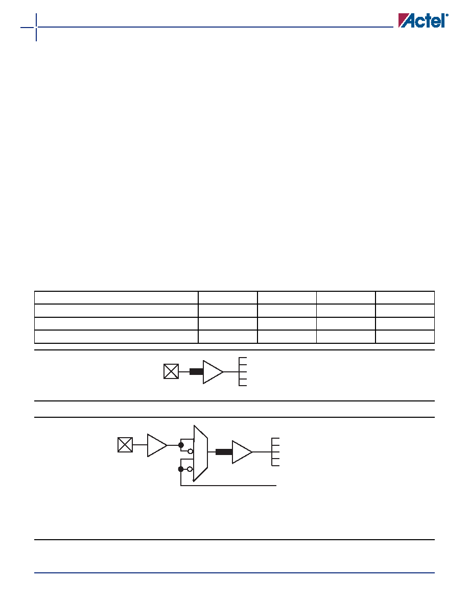
Figure 1-7 SX-A HCLK Clock Buffer
Figure 1-8 SX-A Routed Clock Buffer
Constant Load
Clock Network
HCLKBUF
Clock Network
From Internal Logic
CLKBUF
CLKBUFI
CLKINT
CLKINTI
相关PDF资料 |
PDF描述 |
|---|---|
| A54SX08A-2TQG144I | IC FPGA SX 12K GATES 144-TQFP |
| A3P250-1FGG144T | IC FPGA 1KB FLASH 250K 144-FBGA |
| A3P250-1FG144T | IC FPGA 1KB FLASH 250K 144-FBGA |
| EP4CE40F23C9LN | IC CYCLONE IV FPGA 40K 484FBGA |
| EP4CE40F23C8N | IC CYCLONE IV FPGA 40K 484FBGA |
相关代理商/技术参数 |
参数描述 |
|---|---|
| A54SX08A-2TQ208 | 制造商:未知厂家 制造商全称:未知厂家 功能描述:SX-A Family FPGAs |
| A54SX08A-2TQ208A | 制造商:未知厂家 制造商全称:未知厂家 功能描述:SX-A Family FPGAs |
| A54SX08A-2TQ208B | 制造商:未知厂家 制造商全称:未知厂家 功能描述:SX-A Family FPGAs |
| A54SX08A-2TQ208I | 制造商:未知厂家 制造商全称:未知厂家 功能描述:SX-A Family FPGAs |
| A54SX08A-2TQ208M | 制造商:未知厂家 制造商全称:未知厂家 功能描述:SX-A Family FPGAs |
发布紧急采购,3分钟左右您将得到回复。