- 您现在的位置:买卖IC网 > PDF目录379534 > A54SX08P-TQ208 (Electronic Theatre Controls, Inc.) LM1881 Video Sync Separator; Package: MDIP; No of Pins: 8; Qty per Container: 40; Container: Rail PDF资料下载
参数资料
| 型号: | A54SX08P-TQ208 |
| 厂商: | Electronic Theatre Controls, Inc. |
| 英文描述: | LM1881 Video Sync Separator; Package: MDIP; No of Pins: 8; Qty per Container: 40; Container: Rail |
| 中文描述: | 54SX家庭的FPGA |
| 文件页数: | 8/57页 |
| 文件大小: | 415K |
| 代理商: | A54SX08P-TQ208 |
第1页第2页第3页第4页第5页第6页第7页当前第8页第9页第10页第11页第12页第13页第14页第15页第16页第17页第18页第19页第20页第21页第22页第23页第24页第25页第26页第27页第28页第29页第30页第31页第32页第33页第34页第35页第36页第37页第38页第39页第40页第41页第42页第43页第44页第45页第46页第47页第48页第49页第50页第51页第52页第53页第54页第55页第56页第57页
5 4 S X F a m ily F P G A s
8
v3.1
P e rform a nc e
The combination of architectural features described above
enables SX devices to operate with internal clock
frequencies exceeding 300 MHz, enabling very fast
execution of even complex logic functions. Thus, the SX
family is an optimal platform upon which to integrate the
functionality previously contained in multiple CPLDs. In
addition, designs that previously would have required a gate
array to meet performance goals can now be integrated into
an SX device with dramatic improvements in cost and time
to market. Using timing-driven place and route tools,
designers can achieve highly deterministic device
performance. With SX devices, designers do not need to use
complicated performance-enhancing design techniques
such as the use of redundant logic to reduce fanout on
critical nets or the instantiation of macros in HDL code to
achieve high performance.
I/O Module s
Each I/O on an SX device can be configured as an input, an
output, a tristate output, or a bidirectional pin. Even without
the inclusion of dedicated I/O registers, these I/Os, in
combination with array registers, can achieve clock-to-out
(pad-to-pad) timing as fast as 3.7 ns. I/O cells that have
embedded latches and flip-flops require instantiation in
HDL code; this is a design complication not encountered in
SX FPGAs. Fast pin-to-pin timing ensures that the device
will have little trouble interfacing with any other device in
the system, which in turn enables parallel design of system
components and reduces overall design time.
P ow e r R e quire m e nt s
The SX family supports 3.3V operation and is designed to
tolerate 5.0V inputs. (
Table1
). Power consumption is
extremely low due to the very short distances signals are
required to travel to complete a circuit. Power requirements
are further reduced because of the small number of
low-resistance antifuses in the path. The antifuse
architecture does not require active circuitry to hold a
charge (as do SRAM or EPROM), making it the lowest-power
architecture on the market.
B ounda ry S c a n T e s t ing (B S T )
All SX devices are IEEE 1149.1 compliant. SX devices offer
superior diagnostic and testing capabilities by providing
Boundary Scan Testing (BST) and probing capabilities.
These functions are controlled through the special test pins
in conjunction with the program fuse. The functionality of
each pin is described in
Table2
.In the dedicated test mode,
TCK, TDI and TDO are dedicated pins and cannot be used as
regular I/Os. In flexible mode, TMS should be set HIGH
through a pull-up resistor of 10k
. TMS can be pulled LOW
to initiate the test sequence.
The program fuse determines whether the device is in
dedicated or flexible mode. The default (fuse not blown) is
flexible mode. .
De v e lopm e nt T ool S upport
The SX devices are fully supported by Actel’s line of FPGA
development tools, including the Actel DeskTOP series and
Designer Advantage tools. The Actel DeskTOP series is an
integrated design environment for PCs that includes design
entry, simulation, synthesis, and place and route tools.
Designer Advantage, Actel’s suite of FPGA development
point tools for PCs and Workstations, includes the ACTgen
Macro Builder, Designer with DirectTime timing driven
place and route and analysis tools, and device programming
software.
In addition, the SX devices contain ActionProbe circuitry
that provides built-in access to every node in a design,
enabling 100-percent real-time observation and analysis of a
device's internal logic nodes without design iteration. The
probe circuitry is accessed by Silicon Explorer II, an
easy-to-use integrated verification and logic analysis tool
that can sample data at 100MHz (asynchronous) or 66MHz
(synchronous). Silicon Explorer II attaches to a PC’s
standard COM port, turning the PC into a fully functional
18-channel logic analyzer. Silicon Explorer II allows
designers to complete the design verification process at
their desks and reduces verification time from several hours
per cycle to only a few seconds.
Table 1
Supply Voltages
V
CCA
V
CCI
V
CCR
Maximum
Input
Tolerance
Maximum
Output
Drive
A54SX08
A54SX16
A54SX32
3.3V
3.3V
5.0V
5.0V
3.3V
A54SX16-P
3.3V
3.3V
3.3V
3.3V
3.3V
5.0V
3.3V
5.0V
5.0V
3.3V
5.0V
5.0V
3.3V
3.3V
5.0V
Note:
A54SX16-P has three different entries because it is capable of
both a 3.3V and a 5V drive.
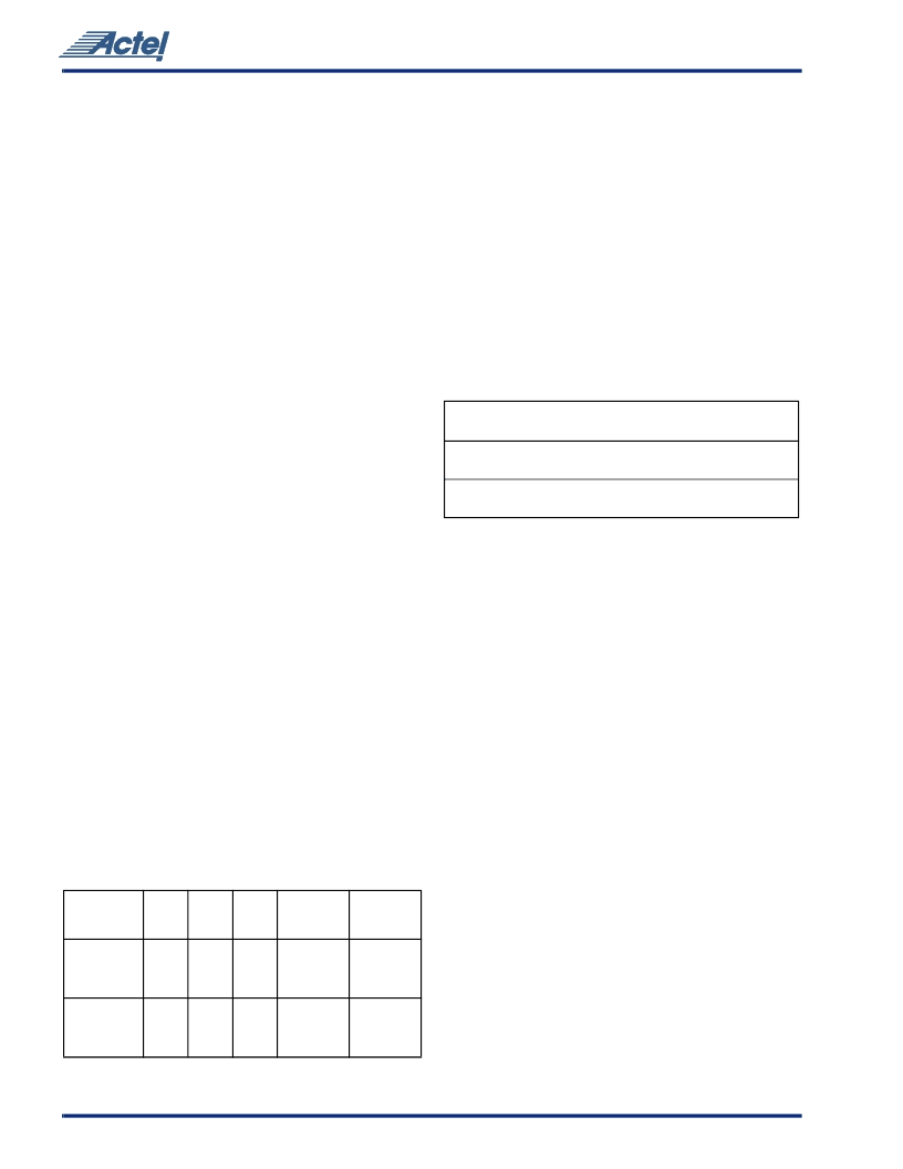
Table 2
Boundary Scan Pin Functionality
Program Fuse Blown
(Dedicated Test Mode)
Program Fuse Not Blown
(Flexible Mode)
TCK, TDI, TDO are
dedicated BST pins
No need for pull-up resistor
for TMS
TCK, TDI, TDO are flexible
and may be used as I/Os
Use a pull-up resistor of 10k
on TMS
相关PDF资料 |
PDF描述 |
|---|---|
| A54SX08P-TQ208I | LM1894 Dynamic Noise Reduction System DNR®; Package: SOIC NARROW; No of Pins: 14; Qty per Container: 55; Container: Rail |
| A54SX08P-TQ208M | 54SX Family FPGAs |
| A54SX08P-TQ208PP | 54SX Family FPGAs |
| A54SX16-2FG208M | 54SX Family FPGAs |
| A54SX16-2FG208PP | 54SX Family FPGAs |
相关代理商/技术参数 |
参数描述 |
|---|---|
| A54SX08P-TQ208I | 制造商:未知厂家 制造商全称:未知厂家 功能描述:54SX Family FPGAs |
| A54SX08P-TQ208M | 制造商:未知厂家 制造商全称:未知厂家 功能描述:54SX Family FPGAs |
| A54SX08P-TQ208PP | 制造商:未知厂家 制造商全称:未知厂家 功能描述:54SX Family FPGAs |
| A54SX08P-VQ208 | 制造商:未知厂家 制造商全称:未知厂家 功能描述:54SX Family FPGAs |
| A54SX08P-VQ208I | 制造商:未知厂家 制造商全称:未知厂家 功能描述:54SX Family FPGAs |
发布紧急采购,3分钟左右您将得到回复。