- 您现在的位置:买卖IC网 > PDF目录10677 > AD1871YRSZ (Analog Devices Inc)IC ADC STEREO AUDIO 24BIT 28SSOP PDF资料下载
参数资料
| 型号: | AD1871YRSZ |
| 厂商: | Analog Devices Inc |
| 文件页数: | 10/28页 |
| 文件大小: | 0K |
| 描述: | IC ADC STEREO AUDIO 24BIT 28SSOP |
| 产品培训模块: | Interfacing AV Converters to Blackfin Processors |
| 标准包装: | 47 |
| 位数: | 24 |
| 采样率(每秒): | 96k |
| 数据接口: | 串行,SPI? |
| 转换器数目: | 2 |
| 电压电源: | 模拟和数字 |
| 工作温度: | -40°C ~ 105°C |
| 安装类型: | 表面贴装 |
| 封装/外壳: | 28-SSOP(0.209",5.30mm 宽) |
| 供应商设备封装: | 28-SSOP |
| 包装: | 管件 |
| 输入数目和类型: | 4 个单端,单极 |
| 产品目录页面: | 777 (CN2011-ZH PDF) |
第1页第2页第3页第4页第5页第6页第7页第8页第9页当前第10页第11页第12页第13页第14页第15页第16页第17页第18页第19页第20页第21页第22页第23页第24页第25页第26页第27页第28页
AD1871
–18–
REV. 0
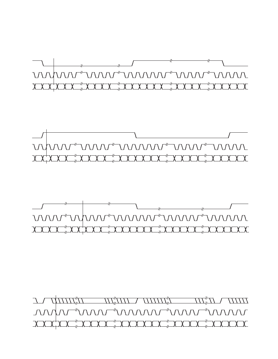
I
2S Mode
In I
2S Mode, the data is left-justified, MSB first, with the MSB
placed in the second BCLK period following the transition of
the LRCLK. A high-to-low transition of the LRCLK signifies
the beginning of the left channel data transfer, while a low-to-
high transition on the LRCLK signifies the beginning of the
right channel data transfer (see Figure 12).
LEFT CHANNEL
RIGHT CHANNEL
MSB–2
MSB–1
LSB+2
LSB+1
LSB
MSB–2
MSB–1
MSB
LSB+2 LSB+1
LSB
MSB
LRCLK
BCLK
DOUT
MSB
Figure 12. I2S Mode
LJ Mode
In LJ Mode, the data is left-justified, MSB first, with the MSB
placed in the first BCLK period following the transition of the
LRCLK. A high-to-low transition of the LRCLK signifies the
beginning of the right channel data transfer, while a low-to-high
transition on the LRCLK signifies the beginning of the left
channel data transfer (see Figure 13).
MSB–2
MSB–1
LSB+2
LSB+1
LSB
MSB–2
MSB–1
MSB
LSB+2
LSB+1
LSB
MSB–1
MSB
LRCLK
BCLK
DOUT
LEFT CHANNEL
RIGHT CHANNEL
MSB
Figure 13. Left-Justified Mode
RJ Mode
In RJ Mode, the data is right-justified, LSB last, with the
LSB placed in the last BCLK period preceding the transition
of the LRCLK. A high-to-low transition of the LRCLK signifies
the beginning of the right channel data transfer, while a low-to-
high transition on the LRCLK signifies the beginning of the left
channel data transfer (see Figure 14).
DOUT
LSB
MSB–2
MSB–1
LSB+2 LSB+1
MSB–2
MSB–1
MSB
LSB+2 LSB+1
LSB
BCLK
LRCLK
LEFT CHANNEL
RIGHT CHANNEL
MSB
LSB
Figure 14. Right-Justified Mode
DSP Mode
In DSP Mode, the LRCLK signal becomes a frame sync signal
that pulses high for the BCLK period prior to the MSB (or in
the BCLK period of the previous LSB–32 bits). The data is left-
justified, MSB first, with the MSB placed in the BCLK period
following the LRCLK pulse (see Figure 15).
In I
2S and LJ Modes, since the data is left-justified, differences in
data word-width between the AD1871 and the controller are not
catastrophic since the MSBs are guaranteed to be transferred.
There may, however, be a slight reduction in performance
depending on the scale of the mismatch. In RJ Mode, however,
differences in word-width between the AD1871 and controller
have a catastrophic effect on signal performance as the MSBs
of each sample may be lost due to the mismatch.
DOUT
MSB–1
LSB+2
LSB+1
LSB
MSB–1
LSB+2
LSB+1
LSB
MSB
MSB–1
MSB
LRCLK
LEFT CHANNEL
RIGHT CHANNEL
BCLK
MSB
Figure 15. DSP Mode
相关PDF资料 |
PDF描述 |
|---|---|
| 1676859-4 | CAP CER 0.82PF 200V 5% NP0 0805 |
| 1676859-3 | CAP CER 0.68PF 200V 5% NP0 0805 |
| 1676859-2 | CAP CER 0.56PF 200V 5% NP0 0805 |
| 1676859-1 | CAP CER 0.47PF 200V 5% NP0 0805 |
| 1676858-4 | CAP CER 0.82PF 100V 5% NP0 0805 |
相关代理商/技术参数 |
参数描述 |
|---|---|
| AD1871YRSZ | 制造商:Analog Devices 功能描述:IC, ADC, 24BIT, 96KHZ, SSOP-28 |
| AD1871YRSZ-REEL | 功能描述:IC ADC STEREO 24BIT 96KHZ 28SSOP RoHS:是 类别:集成电路 (IC) >> 数据采集 - 模数转换器 系列:- 标准包装:1,000 系列:- 位数:16 采样率(每秒):45k 数据接口:串行 转换器数目:2 功率耗散(最大):315mW 电压电源:模拟和数字 工作温度:0°C ~ 70°C 安装类型:表面贴装 封装/外壳:28-SOIC(0.295",7.50mm 宽) 供应商设备封装:28-SOIC W 包装:带卷 (TR) 输入数目和类型:2 个单端,单极 |
| AD1876 | 制造商:AD 制造商全称:Analog Devices 功能描述:16-Bit 100 kSPS Sampling ADC |
| AD1876JN | 制造商:Rochester Electronics LLC 功能描述:- Bulk |
| AD1877 | 制造商:AD 制造商全称:Analog Devices 功能描述:Single-Supply 16-Bit Stereo ADC |
发布紧急采购,3分钟左右您将得到回复。