- 您现在的位置:买卖IC网 > PDF目录10677 > AD1871YRSZ (Analog Devices Inc)IC ADC STEREO AUDIO 24BIT 28SSOP PDF资料下载
参数资料
| 型号: | AD1871YRSZ |
| 厂商: | Analog Devices Inc |
| 文件页数: | 11/28页 |
| 文件大小: | 0K |
| 描述: | IC ADC STEREO AUDIO 24BIT 28SSOP |
| 产品培训模块: | Interfacing AV Converters to Blackfin Processors |
| 标准包装: | 47 |
| 位数: | 24 |
| 采样率(每秒): | 96k |
| 数据接口: | 串行,SPI? |
| 转换器数目: | 2 |
| 电压电源: | 模拟和数字 |
| 工作温度: | -40°C ~ 105°C |
| 安装类型: | 表面贴装 |
| 封装/外壳: | 28-SSOP(0.209",5.30mm 宽) |
| 供应商设备封装: | 28-SSOP |
| 包装: | 管件 |
| 输入数目和类型: | 4 个单端,单极 |
| 产品目录页面: | 777 (CN2011-ZH PDF) |
第1页第2页第3页第4页第5页第6页第7页第8页第9页第10页当前第11页第12页第13页第14页第15页第16页第17页第18页第19页第20页第21页第22页第23页第24页第25页第26页第27页第28页
REV. 0
AD1871
–19–
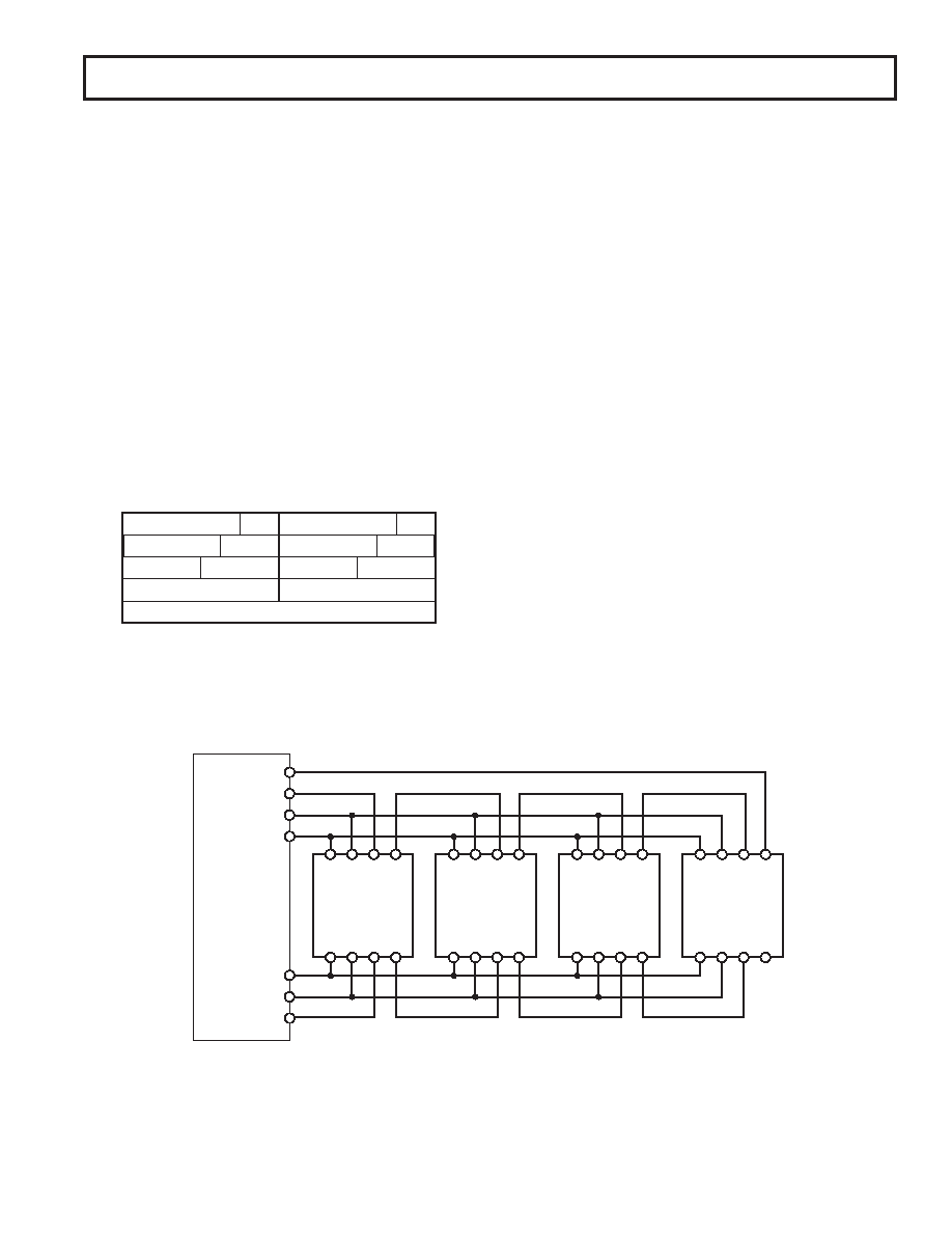
Cascade Mode
The AD1871 supports cascading of up to four devices in a
daisy-chain configuration to the serial port of a DSP. In Cascade
Mode, each device loads an internal 64-Bit Shift Register with
the results of the left and right channel conversions. The 64-
Bit Register is split into two subframes of 32 bits each; the first
for left channel data and the second for right channel data.
The results are left-justified, MSB first within the subframes,
and the word-width setting in Control Register II applies.
Remaining bits within the subframe, beyond the conversion
word-width, are set to zero. Please refer to Figure 16.
Up to four devices can be connected in a daisy chain as shown
in Figure 17. All devices must be set in Cascade Mode by tying
the CASC pin of each device to a logic high. The first device in
the chain (Device 4) has its DIN pin tied to logic low. Its
DOUT pin is connected to the DIN pin of Device 3 whose
DOUT is in turn connected to the DIN pin of Device 2. This
daisy chaining is continued until the DOUT of Device 1 is
connected to the DSP’s serial port RX data line (DR0). The
DSP’s RX serial clock (RXCLK0) is connected to the BCLK
pin of all AD1871 devices and the DSP’s RX frame sync (RFS0)
is connected to the LRCLK pin of all AD1871 devices.
64-BIT FRAME
32-BIT LEFT SUBFRAME
32-BIT RIGHT SUBFRAME
16-BIT RESULT
20-BIT RESULT
24-BIT RESULT
20-BIT RESULT
24-BIT RESULT
Figure 16. DSP Mode
The DSP can be the master and supply the frame sync and
serial clock to the AD1871s, or one of the AD1871s can be
set as the master with the DSP and all other AD1871s set to
slave. Each sampling period begins with a frame sync being gener-
ated either by the DSP or one of the AD1871s, depending on
the
Master/Slave selection. The frame-sync pulse causes each
device to load the 64-Bit Data I/O Register with the left and
right ADC results. These results are then clocked toward the
DSP where they are received in the following order: Device 1,
Left; Device 1, Right; Device 2, Left; Device 2, Right; Device 3,
Left; Device 3, Right; Device 4, Left; and Device 4, Right.
The DSP’s serial port must be programmed to accept 32-bit
word lengths regardless of the AD1871 word length. The number
of sample words to be accepted per sample interval will be
determined by the number of AD1871 devices in cascade, up
to a maximum of eight words corresponding with the maximum
number of four devices.
Figure 17 also shows the connection of a separate DSP serial port
interface to the control port (SPI) interface of the cascaded
AD1871s. Again this cascade is implemented as a daisy chain,
where the control words for the four devices are output in
sequence (depending on the hookup – 1, 2, 3, and 4 in the
example) to be latched simultaneously at each device by the
common CLATCH. In this mode, it is necessary to send a
control word for each device (16 bits
the number of devices)
from the SPI port of the control host. The CLATCH signal can
be controlled from a separate programmable output line. It is
also possible to have individual read/write of the AD1871s
using separate CLATCH controls for each device.
When using Cascade Mode, the data interface defaults to left-
justified, MSB first data, regardless of the state of the Interface
Mode selection (by SPI or external control).
The timing relationships of the Cascade Mode are shown in
Figure 18.
AD1871 No.1
CLATCH
CCLK
COUT
CIN
LRCLK
BCLK
DOUT
DIN
AD1871 No.2
CLATCH
CCLK
COUT
CIN
LRCLK
BCLK
DOUT
DIN
AD1871 No.3
CLATCH
CCLK
COUT
CIN
LRCLK
BCLK
DOUT
DIN
AD1871 No.4
CLATCH
CCLK
COUT
CIN
LRCLK
BCLK
DOUT
DIN
DT1
DR1
TXCLK1/RXCLK1
TFS1/RFS1
RFS0
RXCLK0
DR0
ADSP-21xxx
SHARC DSP
Figure 17. DSP Mode
相关PDF资料 |
PDF描述 |
|---|---|
| 1676859-4 | CAP CER 0.82PF 200V 5% NP0 0805 |
| 1676859-3 | CAP CER 0.68PF 200V 5% NP0 0805 |
| 1676859-2 | CAP CER 0.56PF 200V 5% NP0 0805 |
| 1676859-1 | CAP CER 0.47PF 200V 5% NP0 0805 |
| 1676858-4 | CAP CER 0.82PF 100V 5% NP0 0805 |
相关代理商/技术参数 |
参数描述 |
|---|---|
| AD1871YRSZ | 制造商:Analog Devices 功能描述:IC, ADC, 24BIT, 96KHZ, SSOP-28 |
| AD1871YRSZ-REEL | 功能描述:IC ADC STEREO 24BIT 96KHZ 28SSOP RoHS:是 类别:集成电路 (IC) >> 数据采集 - 模数转换器 系列:- 标准包装:1,000 系列:- 位数:16 采样率(每秒):45k 数据接口:串行 转换器数目:2 功率耗散(最大):315mW 电压电源:模拟和数字 工作温度:0°C ~ 70°C 安装类型:表面贴装 封装/外壳:28-SOIC(0.295",7.50mm 宽) 供应商设备封装:28-SOIC W 包装:带卷 (TR) 输入数目和类型:2 个单端,单极 |
| AD1876 | 制造商:AD 制造商全称:Analog Devices 功能描述:16-Bit 100 kSPS Sampling ADC |
| AD1876JN | 制造商:Rochester Electronics LLC 功能描述:- Bulk |
| AD1877 | 制造商:AD 制造商全称:Analog Devices 功能描述:Single-Supply 16-Bit Stereo ADC |
发布紧急采购,3分钟左右您将得到回复。