- 您现在的位置:买卖IC网 > PDF目录11652 > AD22050RZ-REEL (Analog Devices Inc)IC AMP DIFF SINGLE SUPPLY 8SOIC PDF资料下载
参数资料
| 型号: | AD22050RZ-REEL |
| 厂商: | Analog Devices Inc |
| 文件页数: | 4/8页 |
| 文件大小: | 0K |
| 描述: | IC AMP DIFF SINGLE SUPPLY 8SOIC |
| 产品变化通告: | Product Discontinuance 27/Oct/2011 |
| 标准包装: | 2,500 |
| 类型: | 传感器接口 |
| 输入类型: | 电压 |
| 输出类型: | 模拟 |
| 接口: | 差分 |
| 电流 - 电源: | 200µA |
| 安装类型: | 表面贴装 |
| 封装/外壳: | 8-SOIC(0.154",3.90mm 宽) |
| 供应商设备封装: | 8-SOIC |
| 包装: | 带卷 (TR) |
AD22050
–4–
REV. C
is given by (10 M
/R)%. Thus, the adjustment range would be
±2% for R = 5 M; ± 10% for R = 1 M, etc.
AD22050
+IN
OFS +VS OUT
–IN GND A1
A2
VDM
VCM
R
(SEE TEXT)
VDM = DIFFERENTIAL VOLTAGE, VCM = COMMOM-MODE VOLTAGE
ANALOG
OUTPUT
GAIN ADJUST
20k
MIN
ANALOG
COMMON
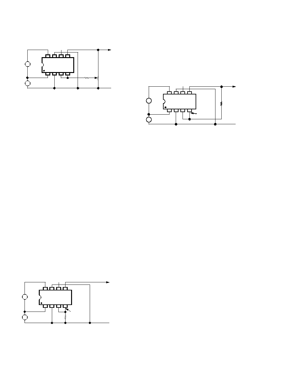
Figure 3. Altering Gain to Accommodate Transducer
Scaling Error
In addition to the method above, another method may be used
to vary the gain. Many applications will call for a gain higher
than
×20, and some require a lower gain. Both of these situa-
tions are readily accommodated by the addition of one external
resistor, plus an optional potentiometer if gain adjustment is
required (for example, to absorb a calibration error in a trans-
ducer).
Decreasing the Gain. See Figure 4. Since the output of the
preamplifier has an output resistance of 100 k
, an external
resistor connected from Pin 4 to ground will precisely lower the
gain by a factor R/(100k+R). When configuring the AD22050
for any gain, the maximum input and the power supply being
used should be considered, since either the preamplifier or the
output buffer will reach its full-scale output (approximately
VS – 0.2 V) with large differential input voltages. The input of
the AD22050 is limited to no greater than (V – 0.2)/10, for
overall gains less than 10, since the preamplifier, with its fixed
gain of
×10, reaches its full scale output before the output
buffer. For VS = 5 V this is 0.48 V. For gains greater than 10,
however, the swing at the buffer output reaches its full-scale first
and limits the AD22050 input to (VS – 0.2)/G, where G is the
overall gain. Increasing the power supply voltage increases the
allowable maximum input. For VS = 5 V and a nominal gain of
20, the maximum input is 240 mV.
The overall bandwidth is unaffected by changes in gain using
this method, although there may be a small offset voltage due to
the imbalance in source resistances at the input to A2. In many
cases this can be ignored but, if desired, can be nulled by insert-
ing a resistor in series with Pin 4 (at “Point X” in Figure 4) of
value 100 k
minus the parallel sum of R and 100 k. For
example, with R = 100 k
(giving a total gain of ×10), the op-
tional offset nulling resistor is 50 k
.
AD22050
+IN
OFS +VS OUT
–IN GND A1
A2
VDM
VCM
R
ANALOG
OUTPUT
ANALOG
COMMON
POINT X
(SEE TEXT)
GAIN = ––––––––
20R
R + 100k
R = 100k –––––––––
GAIN
20 – GAIN
Figure 4. Achieving Gains Less Than
×20
Increasing the Gain. The gain can be raised by connecting a
resistor from the output of the buffer amplifier (Pin 5) to its
noninverting input (Pin 4) as shown in Figure 5. The gain is
now multiplied by the factor R/(R–100k); for example, it is
doubled for R = 200 k
. Overall gains of up to ×160 (R = 114 k)
are readily achievable in this way. Note, however, that the accu-
racy of the gain becomes critically dependent on resistor value at
high gains. Also, the effective input offset voltage at Pins 1 and
8 (about six times the actual offset of A1) limits the part’s use in
very high gain, dc-coupled applications. The gain may be trimmed
by using a fixed and variable resistor in series (see, for example,
Figure 10).
AD22050
+IN OFS +VS OUT
–IN GND A1
A2
VDM
VCM
ANALOG
OUTPUT
ANALOG
COMMON
POINT X
(SEE TEXT)
GAIN = ––––––––
20R
R – 100k
R = 100k –––––––––
GAIN
GAIN – 20
R
Figure 5. Achieving Gains Greater Than
×20
Once again, a small offset voltage will arise from an imbalance
in source resistances and the finite bias currents inherently
present at the input of A2. In most applications this additional
offset error (about 130
V at ×40) will be comparable with the
specified offset range and will therefore introduce negligible
skew. It may, however, be essentially eliminated by the addition
of a resistor in series with the parallel sum of R and 100 k
(i.e., at “Point X” in Figure 5) so the total series resistance is
maintained at 100 k
. For example, at a gain of ×30, when
R = 300 k
and the parallel sum of R and 100 k is 75 k, the
padding resistor should be 25 k
. A 50 k pot would provide
an offset range of about
±2.25 mV referred to the output, or
±75 V referred to the attenuator input. A specific example is
shown in Figure 12.
LOW-PASS FILTERING
In many transducer applications it is necessary to filter the sig-
nal to remove spurious high frequency components, including
noise, or to extract the mean value of a fluctuating signal with a
peak-to-average ratio (PAR) greater than unity. For example, a
full wave rectified sinusoid has a PAR of 1.57, a raised cosine
has a PAR of 2 and a half wave sinusoid has a PAR of 3.14.
Signals having large spikes may have PARs of 10 or more.
When implementing a filter, the PAR should be considered so
the output of the AD22050 preamplifier (A1) does not clip
before A2 does, since this nonlinearity would be averaged and
appear as an error at the output. To avoid this error both ampli-
fiers should be made to clip at the same time. This condition is
achieved when the PAR is no greater than the gain of the second
amplifier (2 for the default configuration). For example, if a
PAR of 5 is expected, the gain of A2 should be increased to 5.
Low-pass filters can be implemented in several ways using the
features provided by the AD22050. In the simplest case, a
single-pole filter (20 dB/decade) is formed when the output of
A1 is connected to the input of A2 via the internal 100 k
resis-
tor by strapping Pins 3 and 4, and a capacitor added from this
node to ground, as shown in Figure 6. The dc gain remains
×20,
and the gain trim shown in Figure 3 may still be used. If a resis-
tor is added across the capacitor to lower the gain, the corner
frequency will increase; it should be calculated using the parallel
sum of the resistor and 100 k
.
相关PDF资料 |
PDF描述 |
|---|---|
| VI-JN1-IY-F3 | CONVERTER MOD DC/DC 12V 50W |
| VI-JN1-IY-F2 | CONVERTER MOD DC/DC 12V 50W |
| D38999/20KB99SN | CONN RCPT 7POS WALL MNT W/SCKT |
| VI-JN1-IY-F1 | CONVERTER MOD DC/DC 12V 50W |
| VI-JN0-IZ-B1 | CONVERTER MOD DC/DC 5V 25W |
相关代理商/技术参数 |
参数描述 |
|---|---|
| AD22050RZ-REEL7 | 功能描述:IC AMP DIFF SINGLE SUPPLY 8SOIC RoHS:是 类别:集成电路 (IC) >> 接口 - 传感器和探测器接口 系列:- 其它有关文件:Automotive Product Guide 产品培训模块:Lead (SnPb) Finish for COTS Obsolescence Mitigation Program 标准包装:74 系列:- 类型:触控式传感器 输入类型:数字 输出类型:数字 接口:JTAG,串行 电流 - 电源:100µA 安装类型:表面贴装 封装/外壳:20-TSSOP(0.173",4.40mm 宽) 供应商设备封装:20-TSSOP 包装:管件 |
| AD22055 | 制造商:AD 制造商全称:Analog Devices 功能描述:Single Supply Bridge Transducer Amplifier |
| AD22055N | 制造商:AD 制造商全称:Analog Devices 功能描述:Single Supply Bridge Transducer Amplifier |
| AD22055R | 制造商:AD 制造商全称:Analog Devices 功能描述:Single Supply Bridge Transducer Amplifier |
| AD22057 | 制造商:AD 制造商全称:Analog Devices 功能描述:Single-Supply Sensor Interface Amplifier |
发布紧急采购,3分钟左右您将得到回复。