- 您现在的位置:买卖IC网 > PDF目录11652 > AD22050RZ-REEL (Analog Devices Inc)IC AMP DIFF SINGLE SUPPLY 8SOIC PDF资料下载
参数资料
| 型号: | AD22050RZ-REEL |
| 厂商: | Analog Devices Inc |
| 文件页数: | 7/8页 |
| 文件大小: | 0K |
| 描述: | IC AMP DIFF SINGLE SUPPLY 8SOIC |
| 产品变化通告: | Product Discontinuance 27/Oct/2011 |
| 标准包装: | 2,500 |
| 类型: | 传感器接口 |
| 输入类型: | 电压 |
| 输出类型: | 模拟 |
| 接口: | 差分 |
| 电流 - 电源: | 200µA |
| 安装类型: | 表面贴装 |
| 封装/外壳: | 8-SOIC(0.154",3.90mm 宽) |
| 供应商设备封装: | 8-SOIC |
| 包装: | 带卷 (TR) |
AD22050
–7–
REV. C
network helps to absorb the additional charge, effectively lower-
ing the high frequency output impedance of the AD22050. For
these applications the output signal should be taken from the
midpoint of the RLAG–CLAG combination as shown in Figure 15.
Since the perturbations from the analog-to-digital converter are
small, the output of the AD22050 will appear to be a low
impedance. The transient response will, therefore, have a
time constant governed by the product of the two lag compo-
nents, CLAG
× R
LAG. For the values shown in Figure 15, this
time constant is programmed at approximately 10
s. There-
fore, if samples are taken at several tens of microseconds or more,
there will be negligible “stacking up” of the charge injections.
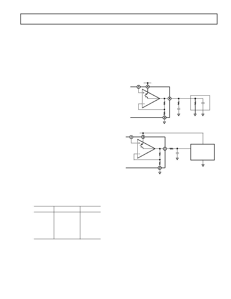
10k
+VS
10k
LOAD
AD22050
A2
RLAG
CLAG
RL
CL
Figure 14. Using an R-C Network for Compensation
0.01 F
1k
10k
+VS
10k
AD22050
A2
PROCESSOR
A/D
IN
Figure 15. Recommended Circuit for Driving CMOS A/D
Converters
UNDERSTANDING THE AD22050
Figure 16 shows the main elements of the AD22050. The signal
inputs at Pins 1 and 8 are first applied to dual resistive attenua-
tors R1 through R4, whose purpose is to reduce the common-
mode voltage at the input to the preamplifier. The attenuated
signal is then applied to a feedback amplifier based on the very
low drift op amp, A1. The differential voltage across the inputs
is accurately amplified in the presence of common-mode volt-
ages of many times the supply voltage. The overall common-
mode response is minimized by precise laser trimming of R3
and R4, giving the AD22050 a common-mode rejection ratio
(CMRR) of at least 80 dB (10,000:1).
The common-mode range of A1 extends from slightly below
ground to 1 V below +VS (at the minimum temperature of
–40
°C). Since an attenuation ratio of about 6 is used, the input
common-mode range is –1 V to +24 V using a +5 V supply.
Small filter capacitors C1 and C2 are included to minimize the
effects of spurious RF signals at the inputs, which might cause
dc errors due to the rectification effects at the input to A1. At
high frequencies, even a small imbalance in these components
would seriously degrade the CMRR, so a special high frequency
trim is also carried out during manufacture.
APPLICATION HINTS
Frequency Compensation
As are all closed-loop op amp circuits, the AD22050 is sensi-
tive to capacitive loading at its output. However, the AD22050
is sensitive at higher output voltages due to nonlinear effects in
the rail-to-rail design of the buffer amplifier (A2). In this
amplifier the output stage gain increases with increasing output
voltage. This behavior does not affect dc parameters such as
gain accuracy or linearity; however, it can compromise ac sta-
bility. When operating from a power supply of 5 V or less (and,
therefore, VOUT < 5 V), the AD22050 can drive capacitive
loads up to 25 pF with no external components. When operat-
ing at higher supply voltages (which are associated with higher
output voltages) and/or driving larger capacitive loads, an ex-
ternal compensation network should be used. Figure 14 shows
an R-C “snubber” circuit loading the output of the AD22050.
This combination, in conjunction with the internal 20 k
resis-
tance, forms a lag network. This network attenuates the open-
loop gain of the amplifier at higher frequencies. The ratio of
RLAG to the load seen by the AD22050 determines the high
frequency attenuation seen by the op amp. If RLAG is made 1/
20th of the total load resistance (
≈20 k R
L), then 26 dB of
attenuation is obtained at higher frequencies. The capacitor
(CLAG) is used to control the frequency of the compensation
network. It should be set to form a 5
s time constant with the
resistor (RLAG). Table I shows the recommended values of
RLAG and CLAG for various values of external load resistor RL.
Ten percent tolerance on these components is acceptable.
Alternatively, the signal may be taken from the midpoint of
RLAG–CLAG. This output is particularly useful when driving
CMOS analog-to-digital converters. For more information see
the section Driving Charged Redistributed A/D Converters.
Note that when implementing this network large signal re-
sponse is compromised. This occurs because there is no active
pull-down and the lag capacitor must discharge through the
internal feedback resistor (20 k
) giving a fairly long-time
constant. For example if CLAG = 0.01
F, the large signal nega-
tive slew characteristic is a decaying exponential with a time
constant of
≈200 s.
Table I. Compensation Components vs. External Load
Resistor
RL
RLAG
CLAG
>100 k
470
0.01
F
> 50 k
390
0.01
F
> 20 k
270
0.047
F
> 10 k
200
0.047
F
> 5 k
100
0.1
F
> 2 k
47
0.22
F
Driving Charge Redistribution A/D Converters
When driving CMOS ADCs, such as those embedded in popu-
lar microcontrollers, the charge injection (
Q) can cause a
significant deflection in the AD22050 output voltage. Though
generally of short duration, this deflection may persist until
after the sample period of the ADC has expired. It is due to the
relatively high open-loop output impedance of the AD22050.
The effect can be significantly reduced by including the same
R-C network recommended for improving stability (see Fre-
quency Compensation section). The large capacitor in the lag
相关PDF资料 |
PDF描述 |
|---|---|
| VI-JN1-IY-F3 | CONVERTER MOD DC/DC 12V 50W |
| VI-JN1-IY-F2 | CONVERTER MOD DC/DC 12V 50W |
| D38999/20KB99SN | CONN RCPT 7POS WALL MNT W/SCKT |
| VI-JN1-IY-F1 | CONVERTER MOD DC/DC 12V 50W |
| VI-JN0-IZ-B1 | CONVERTER MOD DC/DC 5V 25W |
相关代理商/技术参数 |
参数描述 |
|---|---|
| AD22050RZ-REEL7 | 功能描述:IC AMP DIFF SINGLE SUPPLY 8SOIC RoHS:是 类别:集成电路 (IC) >> 接口 - 传感器和探测器接口 系列:- 其它有关文件:Automotive Product Guide 产品培训模块:Lead (SnPb) Finish for COTS Obsolescence Mitigation Program 标准包装:74 系列:- 类型:触控式传感器 输入类型:数字 输出类型:数字 接口:JTAG,串行 电流 - 电源:100µA 安装类型:表面贴装 封装/外壳:20-TSSOP(0.173",4.40mm 宽) 供应商设备封装:20-TSSOP 包装:管件 |
| AD22055 | 制造商:AD 制造商全称:Analog Devices 功能描述:Single Supply Bridge Transducer Amplifier |
| AD22055N | 制造商:AD 制造商全称:Analog Devices 功能描述:Single Supply Bridge Transducer Amplifier |
| AD22055R | 制造商:AD 制造商全称:Analog Devices 功能描述:Single Supply Bridge Transducer Amplifier |
| AD22057 | 制造商:AD 制造商全称:Analog Devices 功能描述:Single-Supply Sensor Interface Amplifier |
发布紧急采购,3分钟左右您将得到回复。