- 您现在的位置:买卖IC网 > PDF目录11652 > AD22050RZ-REEL (Analog Devices Inc)IC AMP DIFF SINGLE SUPPLY 8SOIC PDF资料下载
参数资料
| 型号: | AD22050RZ-REEL |
| 厂商: | Analog Devices Inc |
| 文件页数: | 8/8页 |
| 文件大小: | 0K |
| 描述: | IC AMP DIFF SINGLE SUPPLY 8SOIC |
| 产品变化通告: | Product Discontinuance 27/Oct/2011 |
| 标准包装: | 2,500 |
| 类型: | 传感器接口 |
| 输入类型: | 电压 |
| 输出类型: | 模拟 |
| 接口: | 差分 |
| 电流 - 电源: | 200µA |
| 安装类型: | 表面贴装 |
| 封装/外壳: | 8-SOIC(0.154",3.90mm 宽) |
| 供应商设备封装: | 8-SOIC |
| 包装: | 带卷 (TR) |
AD22050
–8–
REV. C
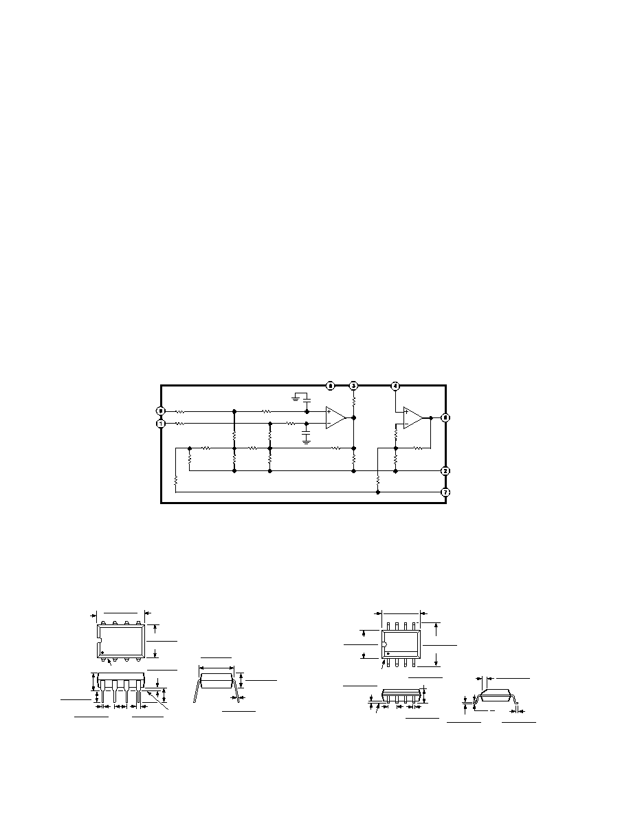
A unique method of feedback around A1, provided by R9 and
R7, sets the closed-loop gain of the preamplifier to
×10 (from
the input pins). The feedback network is balanced by the inclu-
sion of R6 and R8. The small value of R7 results in a more
practical value for R9 (which would have to be 2 M
if the
feedback were taken directly to the inputs of A1). R8 is not
directly connected to ground, but to an optional voltage of one
half that is applied to Pin 7 (OFS). It is trimmed to within
close tolerances through R10 and R11. This allows the output
of A1 to be offset to midscale, typically +VS/2, by tying Pins 6
and 7 together. (For an example of the use of this feature, see
Figure 12.) The gain is adjusted by the single resistor R5,
which acts only on the differential signal. More importantly, it
also results in much less feed forward of the common-mode
signal to the output of A1, which, being a single-supply circuit,
has no means of pulling this output down toward ground in
those circumstances where the common-mode input is very
positive while the net differential signal is small. (The output of
A1 is the collector of a PNP transistor whose emitter is tied to
+VS.) R16 is specifically included to alleviate this problem.
The output of the preamplifier is connected to Pin 3 via R12, a
100 k
resistor that is trimmed to within ±3%. The inclusion
of R12 allows a low-pass filter to be formed, with an accurate
time constant, by placing a capacitor from Pin 3 to ground. By
separating the connections at Pins 3 and 4, a two-pole Sallen
and Key filter can be formed (see Low-Pass Filtering section)
and also provides a means for setting the overall gain to values
other than
×20 (see Altering the Gain section).
The output buffer has a gain of
×2, set by the feedback network
around op amp A2, formed by R15 and R13 R14. Note that this
gain is not trimmed to a precise value, but may have a tolerance
of
±3% (max). Only the overall gain of A1 and A2 is trimmed to
within
±0.5% by R5. As a consequence, the gain of A1 may be
in error by
±3% (max) as the trim to R5 absorbs the initial error
in the gain of A2. In most applications Pins 3 and 4 are simply
tied together, but the output buffer can be used independently if
desired. The offset voltage of A2 is nulled during manufacture.
R17 is included to minimize the offset due to bias currents. It is
recommended, in applications where A2 is used independently
and the source resistance is less than 100 k
, that the necessary
extra resistance should be included.
The output of A2 is the collector of a PNP transistor whose
emitter is tied to +VS. The bias current out of the inverting
input of this amplifier generates an offset voltage of about +1 mV
in R13 R14, which is passed directly to the output via R15. This
sets the lowest output that can be reached when there is no load
resistor. However, the output can drive a 1 k
load to at least
+4.5 V when +VS = +5 V. If operation to much lower minimum
voltages is essential, a load resistor can be added externally.
PRINTED
IN
U.S.A.
AD22050
A1
A2
+VS
R12
100k
A2
C1
5pF
R1
200k
R18
1k
A1
R19 1k
C2
5pF
R4
41k
R9
10k
R7
250
R17
95k
R15
10k
OUT
R16
10k
R14
20k
R13
20k
R5
2.6k
R3
41k
GND
OFS
R6
250k
R8
9k
R2
200k
R11
2k
R10
2k
IN+
IN–
Figure 16. Simplified Schematic of AD22050, Including Component Values
OUTLINE DIMENSIONS
Dimensions shown in inches and (mm).
Plastic SOIC Package
(SO-8)
0.1968 (5.00)
0.1890 (4.80)
8
5
4
1
0.2440 (6.20)
0.2284 (5.80)
PIN 1
0.1574 (4.00)
0.1497 (3.80)
0.0688 (1.75)
0.0532 (1.35)
SEATING
PLANE
0.0098 (0.25)
0.0040 (0.10)
0.0192 (0.49)
0.0138 (0.35)
0.0500
(1.27)
BSC
0.0098 (0.25)
0.0075 (0.19)
0.0500 (1.27)
0.0160 (0.41)
8
0
0.0196 (0.50)
0.0099 (0.25)
45
Plastic Mini-DIP Package
(N-8)
8
14
5
0.430 (10.92)
0.348 (8.84)
0.280 (7.11)
0.240 (6.10)
PIN 1
SEATING
PLANE
0.022 (0.558)
0.014 (0.356)
0.060 (1.52)
0.015 (0.38)
0.210 (5.33)
MAX
0.130
(3.30)
MIN
0.070 (1.77)
0.045 (1.15)
0.100
(2.54)
BSC
0.160 (4.06)
0.115 (2.93)
0.325 (8.25)
0.300 (7.62)
0.015 (0.381)
0.008 (0.204)
0.195 (4.95)
0.115 (2.93)
C1523c–0–3/99
相关PDF资料 |
PDF描述 |
|---|---|
| VI-JN1-IY-F3 | CONVERTER MOD DC/DC 12V 50W |
| VI-JN1-IY-F2 | CONVERTER MOD DC/DC 12V 50W |
| D38999/20KB99SN | CONN RCPT 7POS WALL MNT W/SCKT |
| VI-JN1-IY-F1 | CONVERTER MOD DC/DC 12V 50W |
| VI-JN0-IZ-B1 | CONVERTER MOD DC/DC 5V 25W |
相关代理商/技术参数 |
参数描述 |
|---|---|
| AD22050RZ-REEL7 | 功能描述:IC AMP DIFF SINGLE SUPPLY 8SOIC RoHS:是 类别:集成电路 (IC) >> 接口 - 传感器和探测器接口 系列:- 其它有关文件:Automotive Product Guide 产品培训模块:Lead (SnPb) Finish for COTS Obsolescence Mitigation Program 标准包装:74 系列:- 类型:触控式传感器 输入类型:数字 输出类型:数字 接口:JTAG,串行 电流 - 电源:100µA 安装类型:表面贴装 封装/外壳:20-TSSOP(0.173",4.40mm 宽) 供应商设备封装:20-TSSOP 包装:管件 |
| AD22055 | 制造商:AD 制造商全称:Analog Devices 功能描述:Single Supply Bridge Transducer Amplifier |
| AD22055N | 制造商:AD 制造商全称:Analog Devices 功能描述:Single Supply Bridge Transducer Amplifier |
| AD22055R | 制造商:AD 制造商全称:Analog Devices 功能描述:Single Supply Bridge Transducer Amplifier |
| AD22057 | 制造商:AD 制造商全称:Analog Devices 功能描述:Single-Supply Sensor Interface Amplifier |
发布紧急采购,3分钟左右您将得到回复。