- 您现在的位置:买卖IC网 > PDF目录11652 > AD22050RZ-REEL (Analog Devices Inc)IC AMP DIFF SINGLE SUPPLY 8SOIC PDF资料下载
参数资料
| 型号: | AD22050RZ-REEL |
| 厂商: | Analog Devices Inc |
| 文件页数: | 6/8页 |
| 文件大小: | 0K |
| 描述: | IC AMP DIFF SINGLE SUPPLY 8SOIC |
| 产品变化通告: | Product Discontinuance 27/Oct/2011 |
| 标准包装: | 2,500 |
| 类型: | 传感器接口 |
| 输入类型: | 电压 |
| 输出类型: | 模拟 |
| 接口: | 差分 |
| 电流 - 电源: | 200µA |
| 安装类型: | 表面贴装 |
| 封装/外壳: | 8-SOIC(0.154",3.90mm 宽) |
| 供应商设备封装: | 8-SOIC |
| 包装: | 带卷 (TR) |
AD22050
–6–
REV. C
To produce a full-scale output of +4 V, a gain
×40 is used, adjust-
able by
±5% to absorb the tolerance in the sense resistor. There is
sufficient headroom to allow at least a 10% overrange (to +4.4 V).
The roughly triangular voltage across the sense resistor is aver-
aged by a single-pole low-pass filter, here set with a corner fre-
quency of fC = 3.6 Hz, which provides about 30 dB of attenuation
at 100 Hz. A higher rate of attenuation can be obtained by a
two-pole filter having fC = 20 Hz, as shown in Figure 11. Al-
though this circuit uses two separate capacitors, the total capaci-
tance is less than half that needed for the single-pole filter.
AD22050
+IN
OFS +VS OUT
–IN GND A1
A2
100m
SOLENOID
LOAD
POWER
DARLINGTON
CMOS DRIVER
+VS (BATTERY)
CHASSIS
C
432k
50k
+5V
ANALOG
OUTPUT
CORNER FREQUENCY
= 1Hz- F
(0.05 F FOR fC= 20Hz)
ANALOG
COMMON
FLYBACK
DIODE
127k
C
Figure 11. Illustration of Two-Pole Low-Pass Filtering
STRAIN GAGE INTERFACE: MIDSCALE OFFSET
FEATURE
The AD22050 can be used to interface a strain gage to a subse-
quent process where only a single supply voltage is available. In
this application, the midscale offset feature is valuable, since the
output of the bridge may have either polarity. Figure 12 shows
typical connections.
AD22050
+IN OFS +VS OUT
–IN GND A1
A2
RL
10k
+VS
ANALOG OUTPUT
ANALOG COMMON
100k
VOS NULL
OPTIONAL
LP FILTER
125k
(SETS GAIN
TO
100)
VG
R
Figure 12. Typical Connections for a Strain Gage Interface
Using the Offset Feature
The offset is obtained by connecting Pin 7 (OFS) to the supply
voltage. In this way, the output of the AD22050 is centered to
midway between the supply and ground. In many systems the
supply will also serve as the reference voltage for a subsequent
A/D converter. Alternatively, Pin 7 may be tied to the reference
voltage from an independent source. The AD22050 is trimmed
to guarantee an accuracy of
±2% on the 0.5 ratio between the
voltage on Pin 7 and the output.
An ac excitation of up to
±2 V can also be used because the
common-mode range of the AD22050 extends to –1 V. Assum-
ing a full-scale bridge output (VG) of
±10 mV, a gain of ×100
might be used to provide an output of
±1 V (a full-scale range
of +1.5 V to +3.5 V). This gain is achieved using the method
discussed in connection with Figure 5. Note that the gain-
setting resistor does not affect the accuracy of the midscale
offset. (However, if the gain were lowered, using a resistor to
ground, this offset would no longer be accurate.) A VOS nulling
pot is included for illustrative purposes. One-, two- and three-
pole filtering can also be implemented, as discussed in the
Low-Pass Filtering section.
Using the Midscale Offset Feature
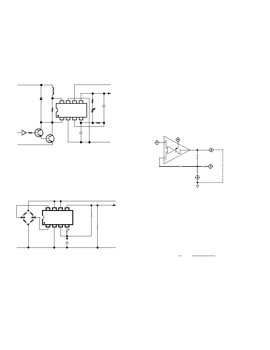
Figure 13 shows a more detailed schematic of the output am-
plifier A2. Because this is a single supply device, the output
stage has no pull-down transistor. Such a transistor would limit
the minimum output to several hundred millivolts above
ground. When using the AD22050 in unipolar mode (Pin 7
grounded), the resistors making up the feedback network also
act as a pull-down for the output stage.
A2
10k
95k
+VS
20k
OFS
OUT
20k
RL
GND
Figure 13. Detailed Schematic of Output Amplifier A2
If the output is called upon to source current (not sink), then it
can swing almost completely to ground (within 20 mV). How-
ever, if the offset pin is connected to some positive voltage
source, this source will “pull up” the output voltage, thereby
limiting the minimum output swing. With no external load the
minimum output voltage possible is VOFS/2. For example, if Pin
7 is connected to +5 V, the minimum output voltage is equal
to the offset voltage of 2.5 V. By adding an additional load, as
shown, the output swing toward ground can be extended.
The relationship is described by:
VOUT >
1
2
VOFS
RL
RL + 20 k *
*This 20 k
resistor is internal to the AD22050 and can vary by ± 30%.
where RL is an externally applied load resistor. However, RL
cannot be made arbitrarily small since this would require exces-
sive current from the output. The output current should be
limited to 5 mA total.
相关PDF资料 |
PDF描述 |
|---|---|
| VI-JN1-IY-F3 | CONVERTER MOD DC/DC 12V 50W |
| VI-JN1-IY-F2 | CONVERTER MOD DC/DC 12V 50W |
| D38999/20KB99SN | CONN RCPT 7POS WALL MNT W/SCKT |
| VI-JN1-IY-F1 | CONVERTER MOD DC/DC 12V 50W |
| VI-JN0-IZ-B1 | CONVERTER MOD DC/DC 5V 25W |
相关代理商/技术参数 |
参数描述 |
|---|---|
| AD22050RZ-REEL7 | 功能描述:IC AMP DIFF SINGLE SUPPLY 8SOIC RoHS:是 类别:集成电路 (IC) >> 接口 - 传感器和探测器接口 系列:- 其它有关文件:Automotive Product Guide 产品培训模块:Lead (SnPb) Finish for COTS Obsolescence Mitigation Program 标准包装:74 系列:- 类型:触控式传感器 输入类型:数字 输出类型:数字 接口:JTAG,串行 电流 - 电源:100µA 安装类型:表面贴装 封装/外壳:20-TSSOP(0.173",4.40mm 宽) 供应商设备封装:20-TSSOP 包装:管件 |
| AD22055 | 制造商:AD 制造商全称:Analog Devices 功能描述:Single Supply Bridge Transducer Amplifier |
| AD22055N | 制造商:AD 制造商全称:Analog Devices 功能描述:Single Supply Bridge Transducer Amplifier |
| AD22055R | 制造商:AD 制造商全称:Analog Devices 功能描述:Single Supply Bridge Transducer Amplifier |
| AD22057 | 制造商:AD 制造商全称:Analog Devices 功能描述:Single-Supply Sensor Interface Amplifier |
发布紧急采购,3分钟左右您将得到回复。