- 您现在的位置:买卖IC网 > PDF目录9310 > AD5161BRM5-RL7 (Analog Devices Inc)IC DGTL POT SPI 256POS 10-MSOP PDF资料下载
参数资料
| 型号: | AD5161BRM5-RL7 |
| 厂商: | Analog Devices Inc |
| 文件页数: | 10/20页 |
| 文件大小: | 0K |
| 描述: | IC DGTL POT SPI 256POS 10-MSOP |
| 标准包装: | 1,000 |
| 接片: | 256 |
| 电阻(欧姆): | 5k |
| 电路数: | 1 |
| 温度系数: | 标准值 45 ppm/°C |
| 存储器类型: | 易失 |
| 接口: | I²C,SPI |
| 电源电压: | 2.7 V ~ 5.5 V |
| 工作温度: | -40°C ~ 125°C |
| 安装类型: | 表面贴装 |
| 封装/外壳: | 10-TFSOP,10-MSOP(0.118",3.00mm 宽) |
| 供应商设备封装: | 10-MSOP |
| 包装: | 带卷 (TR) |
AD5161
Data Sheet
Rev. B | Page 18 of 20
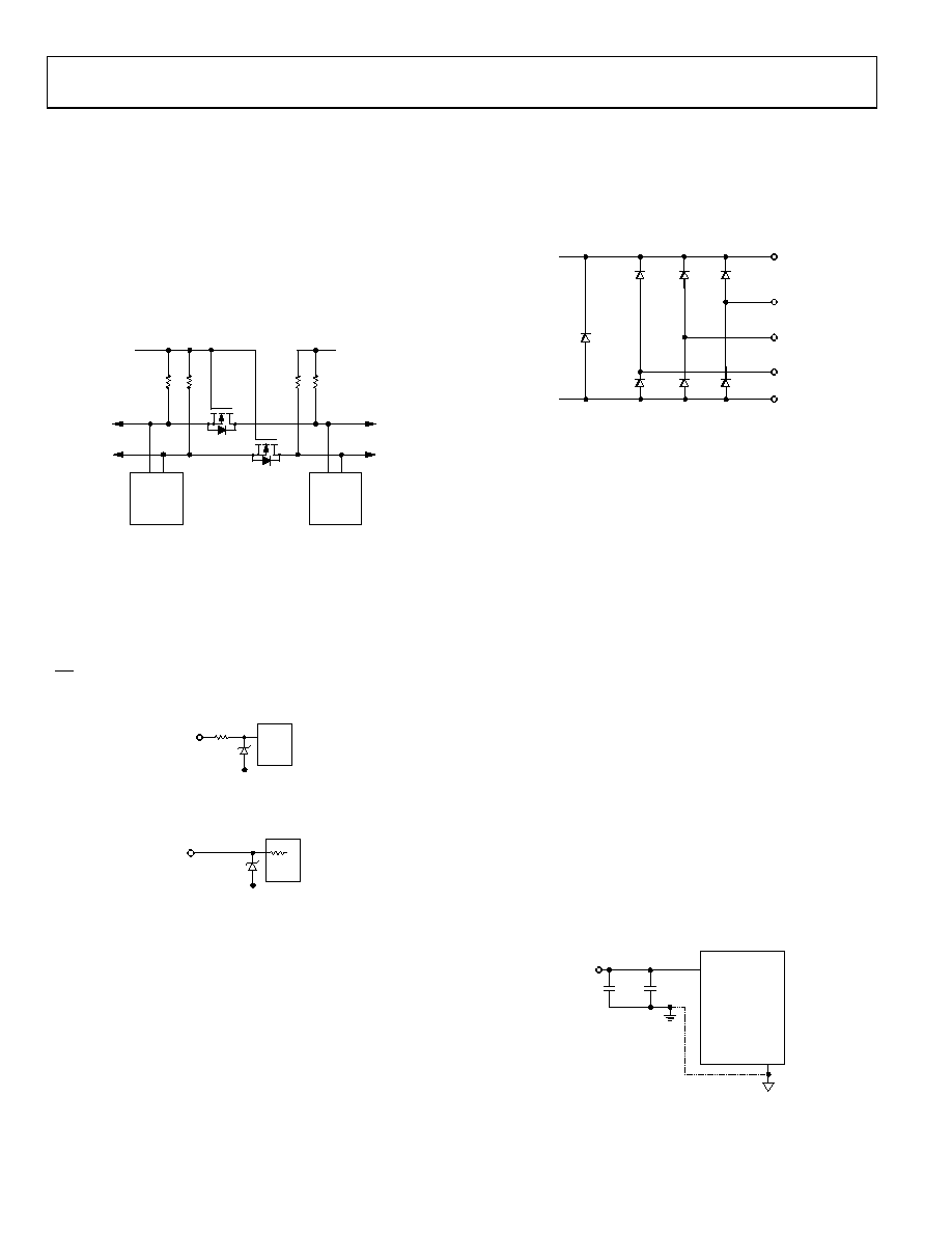
LEVEL SHIFTING FOR BIDIRECTIONAL INTERFACE
While most legacy systems may be operated at one voltage, a
new component may be optimized at another. When two systems
operate the same signal at two different voltages, proper level
shifting is needed. For instance, one can use a 3.3 V E2PROM to
interface with a 5 V digital potentiometer. A level shifting scheme is
needed to enable a bidirectional communication so that the setting
of the digital potentiometer can be stored to and retrieved from
and M2 can be any N-channel signal FETs, or if VDD falls below
2.5 V, low threshold FETs such as the FDV301N.
E2PROM
AD5161
SDA1
SCL1
D
G
RP
3.3V
5V
S
M1
SCL2
SDA2
RP
G
S
M2
VDD1 = 3.3V
VDD2 = 5V
D
Figure 45. Level Shifting for Operation at Different Potentials
ESD PROTECTION
All digital inputs are protected with a series input resistor and
parallel Zener ESD structures shown in Figure 46 and Figure 47.
This applies to the digital input pins SDI/SDA, CLK/SCL, and
CS/AD0.
LOGIC
340
Vss
Figure 46. ESD Protection of Digital Pins
A,B,W
VSS
Figure 47. ESD Protection of Resistor Terminals
TERMINAL VOLTAGE OPERATING RANGE
The AD5161 VDD and GND power supply defines the boundary
conditions for proper 3-terminal digital potentiometer
operation. Supply signals present on terminals A, B, and W that
exceed VDD or GND will be clamped by the internal forward
biased diodes (see Figure 48).
A
VDD
B
W
VSS
Figure 48. Maximum Terminal Voltages Set by VDD and VSS
POWER-UP SEQUENCE
Since the ESD protection diodes limit the voltage compliance at
terminals A, B, and W (see Figure 48), it is important to power
VDD/GND before applying any voltage to terminals A, B, and W;
otherwise, the diode will be forward biased such that VDD will
be powered unintentionally and may affect the rest of the user’s
circuit. The ideal power-up sequence is in the following order:
GND, VDD, digital inputs, and then VA/B/W. The relative order of
powering VA, VB, VW, and the digital inputs is not important as
long as they are powered after VDD/GND.
LAYOUT AND POWER SUPPLY BYPASSING
It is a good practice to employ compact, minimum lead length
layout design. The leads to the inputs should be as direct as
possible with a minimum conductor length. Ground paths
should have low resistance and low inductance.
Similarly, it is also a good practice to bypass the power supplies
with quality capacitors for optimum stability. Supply leads to
the device should be bypassed with disc or chip ceramic
capacitors of 0.01 F to 0.1 F. Low ESR 1 F to 10 F tantalum
or electrolytic capacitors should also be applied at the supplies
to minimize any transient disturbance and low frequency ripple
(see Figure 49). Note that the digital ground should also be
joined remotely to the analog ground at one point to minimize
the ground bounce.
AD5161
VDD
C1
C3
GND
10
F
0.1
F
+
VDD
Figure 49. Power Supply Bypassing
相关PDF资料 |
PDF描述 |
|---|---|
| DS14285S+T&R | IC RTC W/NV RAM CNTRL 24-SOIC |
| DS14285S+ | IC RTC W/NV RAM CNTRL 24-SOIC |
| AD5161BRM100-RL7 | IC DGTL POT SPI 256POS 10-MSOP |
| VE-B6P-IU-F4 | CONVERTER MOD DC/DC 13.8V 200W |
| VE-BWM-MW-B1 | CONVERTER MOD DC/DC 10V 100W |
相关代理商/技术参数 |
参数描述 |
|---|---|
| AD5161BRMZ10 | 功能描述:IC DGTL POT SPI 10K 10-MSOP RoHS:是 类别:集成电路 (IC) >> 数据采集 - 数字电位器 系列:- 产品培训模块:Lead (SnPb) Finish for COTS Obsolescence Mitigation Program 标准包装:1 系列:- 接片:256 电阻(欧姆):100k 电路数:1 温度系数:标准值 35 ppm/°C 存储器类型:非易失 接口:3 线串口 电源电压:2.7 V ~ 5.25 V 工作温度:-40°C ~ 85°C 安装类型:表面贴装 封装/外壳:8-WDFN 裸露焊盘 供应商设备封装:8-TDFN-EP(3x3) 包装:剪切带 (CT) 产品目录页面:1399 (CN2011-ZH PDF) 其它名称:MAX5423ETA+TCT |
| AD5161BRMZ10 | 制造商:Analog Devices 功能描述:IC 8-BIT DIGITAL POT |
| AD5161BRMZ100 | 功能描述:IC DGTL POT SPI 100K 10-MSOP RoHS:是 类别:集成电路 (IC) >> 数据采集 - 数字电位器 系列:- 标准包装:3,300 系列:WiperLock™ 接片:257 电阻(欧姆):100k 电路数:1 温度系数:标准值 150 ppm/°C 存储器类型:易失 接口:3 线 SPI(芯片选择) 电源电压:1.8 V ~ 5.5 V 工作温度:-40°C ~ 125°C 安装类型:表面贴装 封装/外壳:8-VDFN 裸露焊盘 供应商设备封装:8-DFN-EP(3x3) 包装:带卷 (TR) |
| AD5161BRMZ100-RL7 | 功能描述:IC DGTL POT SPI 100K 10-MSOP RoHS:是 类别:集成电路 (IC) >> 数据采集 - 数字电位器 系列:- 标准包装:3,000 系列:DPP 接片:32 电阻(欧姆):10k 电路数:1 温度系数:标准值 300 ppm/°C 存储器类型:非易失 接口:3 线串行(芯片选择,递增,增/减) 电源电压:2.5 V ~ 6 V 工作温度:-40°C ~ 85°C 安装类型:表面贴装 封装/外壳:8-WFDFN 裸露焊盘 供应商设备封装:8-TDFN(2x3) 包装:带卷 (TR) |
| AD5161BRMZ10-RL7 | 功能描述:IC DGTL POT SPI 10K 10-MSOP RoHS:是 类别:集成电路 (IC) >> 数据采集 - 数字电位器 系列:- 标准包装:3,000 系列:DPP 接片:32 电阻(欧姆):10k 电路数:1 温度系数:标准值 300 ppm/°C 存储器类型:非易失 接口:3 线串行(芯片选择,递增,增/减) 电源电压:2.5 V ~ 6 V 工作温度:-40°C ~ 85°C 安装类型:表面贴装 封装/外壳:8-WFDFN 裸露焊盘 供应商设备封装:8-TDFN(2x3) 包装:带卷 (TR) |
发布紧急采购,3分钟左右您将得到回复。