- 您现在的位置:买卖IC网 > PDF目录9310 > AD5161BRM5-RL7 (Analog Devices Inc)IC DGTL POT SPI 256POS 10-MSOP PDF资料下载
参数资料
| 型号: | AD5161BRM5-RL7 |
| 厂商: | Analog Devices Inc |
| 文件页数: | 8/20页 |
| 文件大小: | 0K |
| 描述: | IC DGTL POT SPI 256POS 10-MSOP |
| 标准包装: | 1,000 |
| 接片: | 256 |
| 电阻(欧姆): | 5k |
| 电路数: | 1 |
| 温度系数: | 标准值 45 ppm/°C |
| 存储器类型: | 易失 |
| 接口: | I²C,SPI |
| 电源电压: | 2.7 V ~ 5.5 V |
| 工作温度: | -40°C ~ 125°C |
| 安装类型: | 表面贴装 |
| 封装/外壳: | 10-TFSOP,10-MSOP(0.118",3.00mm 宽) |
| 供应商设备封装: | 10-MSOP |
| 包装: | 带卷 (TR) |
AD5161
Data Sheet
Rev. B | Page 16 of 20
PROGRAMMING THE POTENTIOMETER DIVIDER
Voltage Output Operation
The digital potentiometer easily generates a voltage divider at
wiper-to-B and wiper-to-A proportional to the input voltage at
A-to-B. Unlike the polarity of VDD to GND, which must be
positive, voltage across A-B, W-A, and W-B can be at either
polarity.
If ignoring the effect of the wiper resistance for approximation,
connecting the A terminal to 5 V and the B terminal to ground
produces an output voltage at the wiper-to-B starting at 0 V up
to 1 LSB less than 5 V. Each LSB of voltage is equal to the
voltage applied across terminal AB divided by the 256 positions
of the potentiometer divider. The general equation defining the
output voltage at VW with respect to ground for any valid input
voltage applied to terminals A and B is
B
A
W
V
D
V
D
V
256
)
(
+
=
(3)
For a more accurate calculation, which includes the effect of
wiper resistance, VW, can be found as
B
WA
A
WB
W
V
D
R
V
D
R
D
V
256
)
(
256
)
(
)
(
+
=
(4)
Operation of the digital potentiometer in the divider mode
results in a more accurate operation over temperature. Unlike
the rheostat mode, the output voltage is dependent mainly on
the ratio of the internal resistors RWA and RWB and not the
absolute values. Therefore, the temperature drift reduces to
15 ppm/°C.
PIN SELECTABLE DIGITAL INTERFACE
The AD5161 provides the flexibility of a selectable interface.
When the digital interface select (DIS) pin is tied low, the SPI
mode is engaged. When the DIS pin is tied high, the I2C mode
is engaged.
SPI Compatible 3-Wire Serial Bus (DIS = 0)
The AD5161 contains a 3-wire SPI compatible digital interface
(SDI, CS, and CLK). The 8-bit serial word must be loaded MSB
first. The format of the word is shown in Table 6.
The positive-edge sensitive CLK input requires clean transitions
to avoid clocking incorrect data into the serial input register.
Standard logic families work well. If mechanical switches are
used for product evaluation, they should be debounced by a
flip-flop or other suitable means. When CS is low, the clock
loads data into the serial register on each positive clock edge
The data setup and data hold times in the specification table
determine the valid timing requirements. The AD5161 uses an
8-bit serial input data register word that is transferred to the
internal RDAC register when the CS line returns to logic high.
Extra MSB bits are ignored.
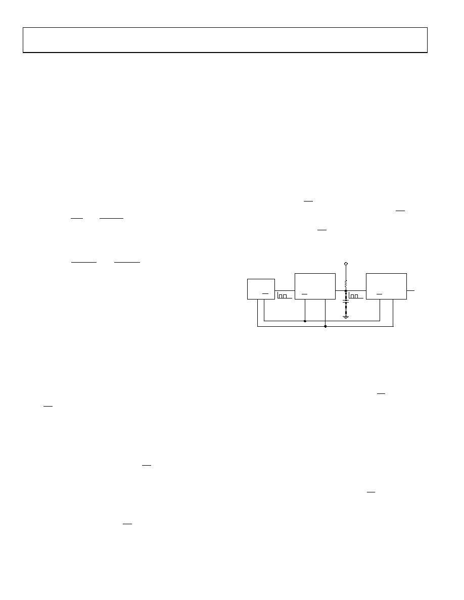
Daisy-Chain Operation
The serial data output (SDO) pin contains an open-drain
N-channel FET. This output requires a pull-up resistor in order
to transfer data to the next package’s SDI pin. This allows for
daisy-chaining several RDACs from a single processor serial
data line. The pull-up resistor termination voltage can be larger
than the VDD supply voltage. It is recommended to increase the
clock period when using a pull-up resistor to the SDI pin of the
following device because capacitive loading at the daisy-chain
node SDO-SDI between devices may induce time delay to
subsequent devices. Users should be aware of this potential
problem to achieve data transfer successfully (see Figure 43). If
two AD5161s are daisy-chained, a total of at least 16 bits of data
is required. The first eight bits, complying with the format
shown in Table 6, go to U2 and the second eight bits with the
same format go to U1. CS should be kept low until all 16 bits are
clocked into their respective serial registers. After this, CS is
pulled high to complete the operation and load the RDAC latch.
If the data word during the CS low period is greater than 16
bits, any additional MSBs will be discarded.
AD5161
U2
C
U1
CS
SDI
CLK
SDO
CS
CLK
SDI
SDO
SC
MOSI
VDD
RP
2.2k
Figure 43. Daisy-Chain Configuration
I2C Compatible 2-Wire Serial Bus (DIS = 1)
The AD5161 can also be controlled via an I2C compatible serial
bus with DIS tied high. The RDACs are connected to this bus as
slave devices.
The first byte of the AD5161 is a slave address byte (see Table 7
and Table 8). It has a 7-bit slave address and a R/W bit. The six
MSBs of the slave address are 010110, and the following bit is
determined by the state of the AD0 pin of the device. AD0
allows the user to place up to two of the I2C compatible devices
on one bus.
The 2-wire I2C serial bus protocol operates as follows:
1. The master initiates data transfer by establishing a START
condition, which is when a high-to-low transition on the
SDA line occurs while SCL is high (see Figure 40). The
following byte is the slave address byte, which consists of
the 7-bit slave address followed by an R/W bit (this bit
determines whether data will be read from or written to
the slave device).
相关PDF资料 |
PDF描述 |
|---|---|
| DS14285S+T&R | IC RTC W/NV RAM CNTRL 24-SOIC |
| DS14285S+ | IC RTC W/NV RAM CNTRL 24-SOIC |
| AD5161BRM100-RL7 | IC DGTL POT SPI 256POS 10-MSOP |
| VE-B6P-IU-F4 | CONVERTER MOD DC/DC 13.8V 200W |
| VE-BWM-MW-B1 | CONVERTER MOD DC/DC 10V 100W |
相关代理商/技术参数 |
参数描述 |
|---|---|
| AD5161BRMZ10 | 功能描述:IC DGTL POT SPI 10K 10-MSOP RoHS:是 类别:集成电路 (IC) >> 数据采集 - 数字电位器 系列:- 产品培训模块:Lead (SnPb) Finish for COTS Obsolescence Mitigation Program 标准包装:1 系列:- 接片:256 电阻(欧姆):100k 电路数:1 温度系数:标准值 35 ppm/°C 存储器类型:非易失 接口:3 线串口 电源电压:2.7 V ~ 5.25 V 工作温度:-40°C ~ 85°C 安装类型:表面贴装 封装/外壳:8-WDFN 裸露焊盘 供应商设备封装:8-TDFN-EP(3x3) 包装:剪切带 (CT) 产品目录页面:1399 (CN2011-ZH PDF) 其它名称:MAX5423ETA+TCT |
| AD5161BRMZ10 | 制造商:Analog Devices 功能描述:IC 8-BIT DIGITAL POT |
| AD5161BRMZ100 | 功能描述:IC DGTL POT SPI 100K 10-MSOP RoHS:是 类别:集成电路 (IC) >> 数据采集 - 数字电位器 系列:- 标准包装:3,300 系列:WiperLock™ 接片:257 电阻(欧姆):100k 电路数:1 温度系数:标准值 150 ppm/°C 存储器类型:易失 接口:3 线 SPI(芯片选择) 电源电压:1.8 V ~ 5.5 V 工作温度:-40°C ~ 125°C 安装类型:表面贴装 封装/外壳:8-VDFN 裸露焊盘 供应商设备封装:8-DFN-EP(3x3) 包装:带卷 (TR) |
| AD5161BRMZ100-RL7 | 功能描述:IC DGTL POT SPI 100K 10-MSOP RoHS:是 类别:集成电路 (IC) >> 数据采集 - 数字电位器 系列:- 标准包装:3,000 系列:DPP 接片:32 电阻(欧姆):10k 电路数:1 温度系数:标准值 300 ppm/°C 存储器类型:非易失 接口:3 线串行(芯片选择,递增,增/减) 电源电压:2.5 V ~ 6 V 工作温度:-40°C ~ 85°C 安装类型:表面贴装 封装/外壳:8-WFDFN 裸露焊盘 供应商设备封装:8-TDFN(2x3) 包装:带卷 (TR) |
| AD5161BRMZ10-RL7 | 功能描述:IC DGTL POT SPI 10K 10-MSOP RoHS:是 类别:集成电路 (IC) >> 数据采集 - 数字电位器 系列:- 标准包装:3,000 系列:DPP 接片:32 电阻(欧姆):10k 电路数:1 温度系数:标准值 300 ppm/°C 存储器类型:非易失 接口:3 线串行(芯片选择,递增,增/减) 电源电压:2.5 V ~ 6 V 工作温度:-40°C ~ 85°C 安装类型:表面贴装 封装/外壳:8-WFDFN 裸露焊盘 供应商设备封装:8-TDFN(2x3) 包装:带卷 (TR) |
发布紧急采购,3分钟左右您将得到回复。