- 您现在的位置:买卖IC网 > PDF目录8746 > AD5310BRMZ-REEL7 (Analog Devices Inc)IC DAC 10BIT R-R W/BUFF 8-MSOP PDF资料下载
参数资料
| 型号: | AD5310BRMZ-REEL7 |
| 厂商: | Analog Devices Inc |
| 文件页数: | 3/16页 |
| 文件大小: | 0K |
| 描述: | IC DAC 10BIT R-R W/BUFF 8-MSOP |
| 产品培训模块: | Data Converter Fundamentals DAC Architectures |
| 标准包装: | 1,000 |
| 设置时间: | 6µs |
| 位数: | 10 |
| 数据接口: | 串行 |
| 转换器数目: | 1 |
| 电压电源: | 单电源 |
| 功率耗散(最大): | 1.25mW |
| 工作温度: | -40°C ~ 105°C |
| 安装类型: | 表面贴装 |
| 封装/外壳: | 8-TSSOP,8-MSOP(0.118",3.00mm 宽) |
| 供应商设备封装: | 8-MSOP |
| 包装: | 带卷 (TR) |
| 输出数目和类型: | 1 电压,单极;1 电压,双极 |
| 采样率(每秒): | 167k |
Data Sheet
AD5310
Rev. B | Page 11 of 16
THEORY OF OPERATION
D/A SECTION
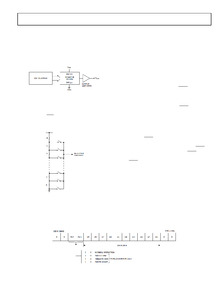
The AD5310 DAC is fabricated on a CMOS process. The
architecture consists of a string DAC followed by an output
buffer amplifier. Because there is no reference input pin, the
block diagram of the DAC architecture.
Figure 23. DAC Architecture
Because the input coding to the DAC is straight binary, the ideal
output voltage is given by
×
=
1024
D
V
DD
OUT
where D is the decimal equivalent of the binary code that is
loaded to the DAC register; it can range from 0 to 1023.
Figure 24. Resistor String
RESISTOR STRING
The resistor string section is shown in Figure 24. It is simply a
string of resistors, each of value R. The code loaded to the DAC
register determines at what node on the string the voltage is
tapped off to be fed into the output amplifier. The voltage is
tapped off by closing one of the switches connecting the string
to the amplifier. Because it is a string of resistors, it is guaranteed
monotonic.
OUTPUT AMPLIFIER
The output buffer amplifier is capable of generating rail-to-rail
voltages on its output, which results in an output range of 0 V to
VDD. It is capable of driving a load of 2 k in parallel with 1000 pF
to GND. The source and sink capabilities of the output amplifier
can be seen in Figure 11 and Figure 12. The slew rate is 1 V/s
with a half-scale settling time of 6 s with the output loaded.
SERIAL INTERFACE
The AD5310 has a 3-wire serial interface (SYNC, SCLK, and
DIN) that is compatible with SPI, QSPI, and MICROWIRE
interface standards, as well as most DSPs. See Figure 2 for a
timing diagram of a typical write sequence.
The write sequence begins by bringing the SYNC line low. Data
from the DIN line is clocked into the 16-bit shift register on the
falling edge of SCLK. The serial clock frequency can be as high
as 30 MHz, making the AD5310 compatible with high speed
DSPs. On the 16th falling clock edge, the last data bit is clocked
in and the programmed function is executed (that is, a change in
DAC register contents and/or a change in the mode of operation).
At this stage, the SYNC line can be kept low or be brought high.
In either case, it must be brought high for a minimum of 33 ns
before the next write sequence so that a falling edge of SYNC
can initiate the next write sequence. Because the SYNC buffer
draws more current when VIN = 2.4 V than it does when VIN =
0.8 V, SYNC should be idled low between write sequences for
even lower power operation of the part. As previously mentioned,
however, it must be brought high again just before the next write
sequence.
INPUT SHIFT REGISTER
The input shift register is 16 bits wide (see Figure 25). The first
two bits are don’t cares. The next two bits are control bits that
control which mode of operation the part is in (normal mode or
one of the three power-down modes). There is a more complete
description of the various modes in the Power-Down Modes
section. The next 10 bits are the data bits. These are transferred
to the DAC register on the 16th falling edge of SCLK. Finally,
the last two bits are don’t cares.
Figure 25. Input Register Contents
相关PDF资料 |
PDF描述 |
|---|---|
| NBSG11MNG | IC CLOCK BUFFER 1:2 12GHZ 16-QFN |
| MC100LVEP210FAG | IC CLOCK BUFFER 1:5 3GHZ 32-LQFP |
| MC100LVE222FAG | IC CLK BUFF DVDR MUX 2:15 52LQFP |
| XRD5410AIDTR-F | IC DAC 10BIT SRL 8SOIC |
| MC100LVEP14DTR2G | IC CLOCK BUFFER MUX 2:5 20-TSSOP |
相关代理商/技术参数 |
参数描述 |
|---|---|
| AD5310BRT | 制造商:Analog Devices 功能描述: |
| AD5310BRT-500RL7 | 功能描述:IC DAC 10BIT R-R W/BUFF SOT23-6 RoHS:否 类别:集成电路 (IC) >> 数据采集 - 数模转换器 系列:- 产品培训模块:Data Converter Fundamentals DAC Architectures 设计资源:Unipolar, Precision DC Digital-to-Analog Conversion using AD5450/1/2/3 8-14-Bit DACs (CN0052) Precision, Bipolar, Configuration for AD5450/1/2/3 8-14bit Multiplying DACs (CN0053) AC Signal Processing Using AD5450/1/2/3 Current Output DACs (CN0054) Programmable Gain Element Using AD5450/1/2/3 Current Output DAC Family (CN0055) Single Supply Low Noise LED Current Source Driver Using a Current Output DAC in the Reverse Mode (CN0139) 标准包装:10,000 系列:- 设置时间:- 位数:12 数据接口:DSP,MICROWIRE?,QSPI?,串行,SPI? 转换器数目:1 电压电源:单电源 功率耗散(最大):- 工作温度:-40°C ~ 125°C 安装类型:表面贴装 封装/外壳:SOT-23-8 薄型,TSOT-23-8 供应商设备封装:TSOT-23-8 包装:带卷 (TR) 输出数目和类型:1 电流,单极;1 电流,双极 采样率(每秒):2.7M |
| AD5310BRT-R2 | 功能描述:INTEGRATED CIRCUIT 制造商:analog devices inc. 系列:* 包装:带卷(TR) 零件状态:最後搶購 封装/外壳:SOT-23-6 供应商器件封装:SOT-23-6 标准包装:1 |
| AD5310BRT-REEL | 功能描述:IC DAC 10BIT R-R W/BUFF SOT23-6 RoHS:否 类别:集成电路 (IC) >> 数据采集 - 数模转换器 系列:- 产品培训模块:Lead (SnPb) Finish for COTS Obsolescence Mitigation Program 标准包装:50 系列:- 设置时间:4µs 位数:12 数据接口:串行 转换器数目:2 电压电源:单电源 功率耗散(最大):- 工作温度:-40°C ~ 85°C 安装类型:表面贴装 封装/外壳:8-TSSOP,8-MSOP(0.118",3.00mm 宽) 供应商设备封装:8-uMAX 包装:管件 输出数目和类型:2 电压,单极 采样率(每秒):* 产品目录页面:1398 (CN2011-ZH PDF) |
| AD5310BRT-REEL7 | 功能描述:IC DAC 10BIT R-R W/BUFF SOT-23 RoHS:否 类别:集成电路 (IC) >> 数据采集 - 数模转换器 系列:- 产品培训模块:Data Converter Fundamentals DAC Architectures 设计资源:Unipolar, Precision DC Digital-to-Analog Conversion using AD5450/1/2/3 8-14-Bit DACs (CN0052) Precision, Bipolar, Configuration for AD5450/1/2/3 8-14bit Multiplying DACs (CN0053) AC Signal Processing Using AD5450/1/2/3 Current Output DACs (CN0054) Programmable Gain Element Using AD5450/1/2/3 Current Output DAC Family (CN0055) Single Supply Low Noise LED Current Source Driver Using a Current Output DAC in the Reverse Mode (CN0139) 标准包装:10,000 系列:- 设置时间:- 位数:12 数据接口:DSP,MICROWIRE?,QSPI?,串行,SPI? 转换器数目:1 电压电源:单电源 功率耗散(最大):- 工作温度:-40°C ~ 125°C 安装类型:表面贴装 封装/外壳:SOT-23-8 薄型,TSOT-23-8 供应商设备封装:TSOT-23-8 包装:带卷 (TR) 输出数目和类型:1 电流,单极;1 电流,双极 采样率(每秒):2.7M |
发布紧急采购,3分钟左右您将得到回复。