- 您现在的位置:买卖IC网 > PDF目录8707 > AD5320BRT-500RL7 (Analog Devices Inc)IC DAC 12BIT R-R W/BUFF SOT23-6 PDF资料下载
参数资料
| 型号: | AD5320BRT-500RL7 |
| 厂商: | Analog Devices Inc |
| 文件页数: | 1/20页 |
| 文件大小: | 0K |
| 描述: | IC DAC 12BIT R-R W/BUFF SOT23-6 |
| 产品培训模块: | Data Converter Fundamentals DAC Architectures |
| 标准包装: | 1 |
| 设置时间: | 8µs |
| 位数: | 12 |
| 数据接口: | DSP,MICROWIRE?,QSPI?,串行,SPI? |
| 转换器数目: | 1 |
| 电压电源: | 单电源 |
| 工作温度: | -40°C ~ 105°C |
| 安装类型: | 表面贴装 |
| 封装/外壳: | SOT-23-6 |
| 供应商设备封装: | SOT-23-6 |
| 包装: | 标准包装 |
| 输出数目和类型: | 1 电压,双极 |
| 采样率(每秒): | 125k |
| 其它名称: | AD5320BRT500RL7DKR |
2.7 V to 5.5 V, 140 μA, Rail-to-Rail Output
12-Bit DAC in an SOT-23
AD5320
Rev. C
Information furnished by Analog Devices is believed to be accurate and reliable. However, no
responsibilityis assumedbyAnalogDevicesforitsuse,norforanyinfringements of patents or other
rightsofthirdpartiesthatmayresultfromitsuse.Specificationssubjecttochangewithoutnotice.No
license is granted by implication or otherwise under any patent or patent rights of Analog Devices.
Trademarksandregisteredtrademarksarethepropertyoftheirrespectiveowners.
One Technology Way, P.O. Box 9106, Norwood, MA 02062-9106, U.S.A.
Tel: 781.329.4700
www.analog.com
Fax: 781.461.3113
2005 Analog Devices, Inc. All rights reserved.
FEATURES
Single 12-bit DAC
6-lead SOT-23 and 8-lead MSOP packages
Micropower operation: 140 μA @ 5 V
Power-down to 200 nA @ 5 V, 50 nA @ 3 V
2.7 V to 5.5 V power supply
Guaranteed monotonic by design
Reference derived from power supply
Power-on reset to zero volts
Three power-down functions
Low power serial interface with Schmitt-triggered inputs
On-chip output buffer amplifier, rail-to-rail operation
SYNC interrupt facility
APPLICATIONS
Portable battery-powered instruments
Digital gain and offset adjustment
Programmable voltage and current sources
Programmable attenuators
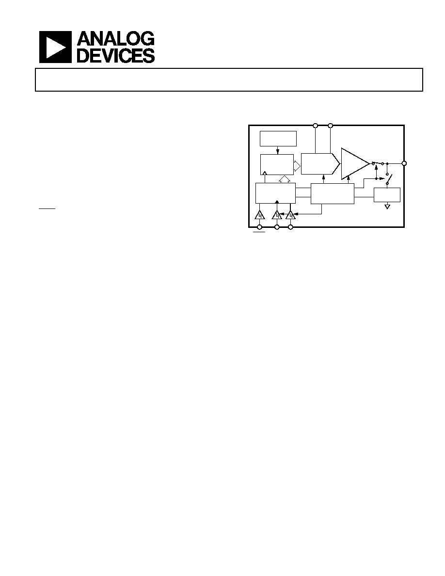
FUNCTIONAL BLOCK DIAGRAM
VDD
VOUT
GND
AD5320
12-BIT
DAC
SCLK DIN
REF (+) REF (–)
REGISTER
NETWORK
POWER-DOWN
CONTROL LOGIC
DAC
REGISTER
OUTPUT
BUFFER
POWER-ON
RESET
SYNC
INPUT
CONTROL
LOGIC
00934
-001
Figure 1.
GENERAL DESCRIPTION
The AD53201 is a single, 12-bit buffered voltage out digital-to-
analog converter (DAC) that operates from a single 2.7 V to
5.5 V supply consuming 115 μA at 3 V. Its on-chip precision
output amplifier allows rail-to-rail output swing to be achieved.
The AD5320 utilizes a versatile 3-wire serial interface that
operates at clock rates up to 30 MHz and is compatible with
standard SPI, QSPI, MICROWIRE and digital signal
processing (DSP) interface standards.
The reference for AD5320 is derived from the power supply
inputs and thus gives the widest dynamic output range. The
part incorporates a power-on reset circuit that ensures that the
DAC output powers up to zero volts and remains there until a
valid write takes place to the device. The part contains a power-
down feature that reduces the current consumption of the
device to 200 nA at 5 V and provides software selectable output
loads while in power-down mode. The part is put into power-
down mode over the serial interface.
The low power consumption of this part in normal operation
makes it ideally suited to portable, battery-operated equipment.
The power consumption is 0.7 mW at 5 V reducing to 1 μW in
power-down mode.
1 Patent pending; protected by U.S. Patent No. 5684481.
The AD5320 is one of a family of pin-compatible DACs. The
AD5300 is the 8-bit version and the AD5310 is the 10-bit
version. The AD5300/AD5310/AD5320 are available in 6-lead
SOT-23 packages and 8-lead MSOP packages.
PRODUCT HIGHLIGHTS
1.
Available in 6-lead SOT-23 and 8-lead MSOP packages.
2.
Low power, single-supply operation. This part operates
from a single 2.7 V to 5.5 V supply and typically consumes
0.35 mW at 3 V and 0.7 mW at 5 V, making it ideal for
battery-powered applications.
3.
The on-chip output buffer amplifier allows the output of
the DAC to swing rail-to-rail with a slew rate of 1 V/μs.
4.
Reference derived from the power supply.
5.
High speed serial interface with clock speeds up to
30 MHz. Designed for very low power consumption. The
interface only powers up during a write cycle.
6.
Power-down capability. When powered down, the DAC
typically consumes 50 nA at 3 V and 200 nA at 5 V.
相关PDF资料 |
PDF描述 |
|---|---|
| VE-JNK-MY | CONVERTER MOD DC/DC 40V 50W |
| VE-JNJ-MY | CONVERTER MOD DC/DC 36V 50W |
| CY28354OXC-400T | IC BUFF 273MHZ 4DDR DIMM 48SSOP |
| VE-BNV-MV-F4 | CONVERTER MOD DC/DC 5.8V 150W |
| IDT2309NZ-1HDCGI8 | IC CLOCK BUFFER 1:9 16-SOIC |
相关代理商/技术参数 |
参数描述 |
|---|---|
| ad5320brt-r2 | 制造商:Rochester Electronics LLC 功能描述:- Bulk 制造商:Analog Devices 功能描述: |
| AD5320BRT-REEL | 功能描述:IC DAC 12BIT R-R W/BUFF SOT-23-6 RoHS:否 类别:集成电路 (IC) >> 数据采集 - 数模转换器 系列:- 产品培训模块:LTC263x 12-, 10-, and 8-Bit VOUT DAC Family 特色产品:LTC2636 - Octal 12-/10-/8-Bit SPI VOUT DACs with 10ppm/°C Reference 标准包装:91 系列:- 设置时间:4µs 位数:10 数据接口:MICROWIRE?,串行,SPI? 转换器数目:8 电压电源:单电源 功率耗散(最大):2.7mW 工作温度:-40°C ~ 85°C 安装类型:表面贴装 封装/外壳:14-WFDFN 裸露焊盘 供应商设备封装:14-DFN-EP(4x3) 包装:管件 输出数目和类型:8 电压,单极 采样率(每秒):* |
| AD5320BRT-REEL7 | 功能描述:IC DAC 12BIT R-R W/BUFF SOT23-6 RoHS:否 类别:集成电路 (IC) >> 数据采集 - 数模转换器 系列:- 产品培训模块:LTC263x 12-, 10-, and 8-Bit VOUT DAC Family 特色产品:LTC2636 - Octal 12-/10-/8-Bit SPI VOUT DACs with 10ppm/°C Reference 标准包装:91 系列:- 设置时间:4µs 位数:10 数据接口:MICROWIRE?,串行,SPI? 转换器数目:8 电压电源:单电源 功率耗散(最大):2.7mW 工作温度:-40°C ~ 85°C 安装类型:表面贴装 封装/外壳:14-WFDFN 裸露焊盘 供应商设备封装:14-DFN-EP(4x3) 包装:管件 输出数目和类型:8 电压,单极 采样率(每秒):* |
| AD5320BRTZ | 制造商:Analog Devices 功能描述:AD5320BRTZ |
| AD5320BRTZ-500RL7 | 功能描述:IC DAC 12BIT R-R W/BUFF SOT23-6 RoHS:是 类别:集成电路 (IC) >> 数据采集 - 数模转换器 系列:- 产品培训模块:LTC263x 12-, 10-, and 8-Bit VOUT DAC Family 特色产品:LTC2636 - Octal 12-/10-/8-Bit SPI VOUT DACs with 10ppm/°C Reference 标准包装:91 系列:- 设置时间:4µs 位数:10 数据接口:MICROWIRE?,串行,SPI? 转换器数目:8 电压电源:单电源 功率耗散(最大):2.7mW 工作温度:-40°C ~ 85°C 安装类型:表面贴装 封装/外壳:14-WFDFN 裸露焊盘 供应商设备封装:14-DFN-EP(4x3) 包装:管件 输出数目和类型:8 电压,单极 采样率(每秒):* |
发布紧急采购,3分钟左右您将得到回复。