- 您现在的位置:买卖IC网 > PDF目录8707 > AD5320BRT-500RL7 (Analog Devices Inc)IC DAC 12BIT R-R W/BUFF SOT23-6 PDF资料下载
参数资料
| 型号: | AD5320BRT-500RL7 |
| 厂商: | Analog Devices Inc |
| 文件页数: | 4/20页 |
| 文件大小: | 0K |
| 描述: | IC DAC 12BIT R-R W/BUFF SOT23-6 |
| 产品培训模块: | Data Converter Fundamentals DAC Architectures |
| 标准包装: | 1 |
| 设置时间: | 8µs |
| 位数: | 12 |
| 数据接口: | DSP,MICROWIRE?,QSPI?,串行,SPI? |
| 转换器数目: | 1 |
| 电压电源: | 单电源 |
| 工作温度: | -40°C ~ 105°C |
| 安装类型: | 表面贴装 |
| 封装/外壳: | SOT-23-6 |
| 供应商设备封装: | SOT-23-6 |
| 包装: | 标准包装 |
| 输出数目和类型: | 1 电压,双极 |
| 采样率(每秒): | 125k |
| 其它名称: | AD5320BRT500RL7DKR |
AD5320
Rev. C | Page 12 of 20
SERIAL INTERFACE
The AD5320 has a 3-wire serial interface (SYNC, SCLK, and
DIN) that is compatible with SPI, QSPITM, and
MICROWIRETM interface standards as well as most DSPs. See
Figure 2 for a timing diagram of a typical write sequence.
The write sequence begins by bringing the SYNC line low. Data
from the DIN line is clocked into the 16-bit shift register on the
falling edge of SCLK. The serial clock frequency can be as high
as 30 MHz, making the AD5320 compatible with high speed
DSPs. On the 16th falling clock edge, the last data bit is clocked
in and the programmed function is executed (that is, a change
in DAC register contents and/or a change in the mode of
operation). At this stage, the SYNC line can be kept low or be
brought high. In either case, it must be brought high for a
minimum of 33 ns before the next write sequence so that a
falling edge of SYNC can initiate the next write sequence.
Because the SYNC buffer draws more current when VIN = 2.4 V
than it does when VIN = 0.8 V, SYNC should be idled low
between write sequences for even lower power operation of the
part. As previously mentioned, SYNC must be brought high
again just before the next write sequence.
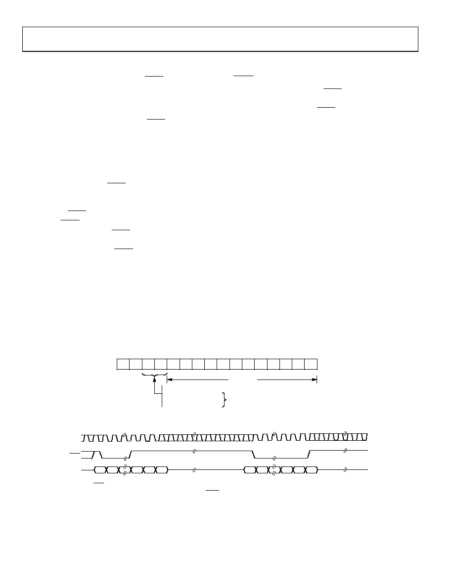
INPUT SHIFT REGISTER
The input shift register is 16 bits wide (see Figure 25). The first two
bits are “don’t cares.” The next two are control bits that control
which mode of operation the part is in (normal mode or any one of
three power-down modes). There is a more complete description of
the various modes in the Power-Down Modes section. The next
twelve bits are the data bits. These are transferred to the DAC
register on the 16th falling edge of SCLK.
SYNC INTERRUPT
In a normal write sequence, the SYNC line is kept low for at
least 16 falling edges of SCLK and the DAC is updated on the
16th falling edge. However, if SYNC is brought high before the
16th falling edge, then this acts as an interrupt to the write
sequence. The shift register is reset and the write sequence is
seen as invalid. Neither an update of the DAC register contents
nor a change in the operating mode occurs (see Figure 26).
POWER-ON RESET
The AD5320 contains a power-on reset circuit that controls the
output voltage during power-up. The DAC register is filled with
zeros and the output voltage is 0 V. It remains there until a valid
write sequence is made to the DAC. This is useful in applica-
tions where it is important to know the state of the output of the
DAC while it is in the process of powering up.
DB15 (MSB)
DB0 (LSB)
X
PD0 D11 D10
D9
D8
D7
D6
D5
D4
PD1
X
D3
D2
D1
D0
DATA BITS
00
93
4-
0
25
0
1
0
1
0
1
NORMAL OPERATION
1k TO GND
100k TO GND
THREE–STATE
POWER-DOWN MODES
Figure 25. Input Register Contents
DB15
DB0
DB15
SCLK
SYNC
DIN
INVALID WRITE SEQUENCE:
SYNC HIGH BEFORE 16TH FALLING EDGE
VALID WRITE SEQUENCE, OUTPUT UPDATES
ON THE 16TH FALLING EDGE
DB0
00934-
028
Figure 26. SYNC Interrupt Facility
相关PDF资料 |
PDF描述 |
|---|---|
| VE-JNK-MY | CONVERTER MOD DC/DC 40V 50W |
| VE-JNJ-MY | CONVERTER MOD DC/DC 36V 50W |
| CY28354OXC-400T | IC BUFF 273MHZ 4DDR DIMM 48SSOP |
| VE-BNV-MV-F4 | CONVERTER MOD DC/DC 5.8V 150W |
| IDT2309NZ-1HDCGI8 | IC CLOCK BUFFER 1:9 16-SOIC |
相关代理商/技术参数 |
参数描述 |
|---|---|
| ad5320brt-r2 | 制造商:Rochester Electronics LLC 功能描述:- Bulk 制造商:Analog Devices 功能描述: |
| AD5320BRT-REEL | 功能描述:IC DAC 12BIT R-R W/BUFF SOT-23-6 RoHS:否 类别:集成电路 (IC) >> 数据采集 - 数模转换器 系列:- 产品培训模块:LTC263x 12-, 10-, and 8-Bit VOUT DAC Family 特色产品:LTC2636 - Octal 12-/10-/8-Bit SPI VOUT DACs with 10ppm/°C Reference 标准包装:91 系列:- 设置时间:4µs 位数:10 数据接口:MICROWIRE?,串行,SPI? 转换器数目:8 电压电源:单电源 功率耗散(最大):2.7mW 工作温度:-40°C ~ 85°C 安装类型:表面贴装 封装/外壳:14-WFDFN 裸露焊盘 供应商设备封装:14-DFN-EP(4x3) 包装:管件 输出数目和类型:8 电压,单极 采样率(每秒):* |
| AD5320BRT-REEL7 | 功能描述:IC DAC 12BIT R-R W/BUFF SOT23-6 RoHS:否 类别:集成电路 (IC) >> 数据采集 - 数模转换器 系列:- 产品培训模块:LTC263x 12-, 10-, and 8-Bit VOUT DAC Family 特色产品:LTC2636 - Octal 12-/10-/8-Bit SPI VOUT DACs with 10ppm/°C Reference 标准包装:91 系列:- 设置时间:4µs 位数:10 数据接口:MICROWIRE?,串行,SPI? 转换器数目:8 电压电源:单电源 功率耗散(最大):2.7mW 工作温度:-40°C ~ 85°C 安装类型:表面贴装 封装/外壳:14-WFDFN 裸露焊盘 供应商设备封装:14-DFN-EP(4x3) 包装:管件 输出数目和类型:8 电压,单极 采样率(每秒):* |
| AD5320BRTZ | 制造商:Analog Devices 功能描述:AD5320BRTZ |
| AD5320BRTZ-500RL7 | 功能描述:IC DAC 12BIT R-R W/BUFF SOT23-6 RoHS:是 类别:集成电路 (IC) >> 数据采集 - 数模转换器 系列:- 产品培训模块:LTC263x 12-, 10-, and 8-Bit VOUT DAC Family 特色产品:LTC2636 - Octal 12-/10-/8-Bit SPI VOUT DACs with 10ppm/°C Reference 标准包装:91 系列:- 设置时间:4µs 位数:10 数据接口:MICROWIRE?,串行,SPI? 转换器数目:8 电压电源:单电源 功率耗散(最大):2.7mW 工作温度:-40°C ~ 85°C 安装类型:表面贴装 封装/外壳:14-WFDFN 裸露焊盘 供应商设备封装:14-DFN-EP(4x3) 包装:管件 输出数目和类型:8 电压,单极 采样率(每秒):* |
发布紧急采购,3分钟左右您将得到回复。