- 您现在的位置:买卖IC网 > PDF目录8742 > AD5428YRUZ-REEL (Analog Devices Inc)IC DAC 8BIT MULTIPLYING 20TSSOP PDF资料下载
参数资料
| 型号: | AD5428YRUZ-REEL |
| 厂商: | Analog Devices Inc |
| 文件页数: | 11/33页 |
| 文件大小: | 0K |
| 描述: | IC DAC 8BIT MULTIPLYING 20TSSOP |
| 产品培训模块: | Data Converter Fundamentals DAC Architectures |
| 标准包装: | 2,500 |
| 设置时间: | 30ns |
| 位数: | 8 |
| 数据接口: | 并联 |
| 转换器数目: | 2 |
| 电压电源: | 单电源 |
| 功率耗散(最大): | 3.3µW |
| 工作温度: | -40°C ~ 125°C |
| 安装类型: | 表面贴装 |
| 封装/外壳: | 20-TSSOP(0.173",4.40mm 宽) |
| 供应商设备封装: | 20-TSSOP |
| 包装: | 带卷 (TR) |
| 输出数目和类型: | 2 电流,单极;2 电流,双极 |
| 采样率(每秒): | 21.3M |
第1页第2页第3页第4页第5页第6页第7页第8页第9页第10页当前第11页第12页第13页第14页第15页第16页第17页第18页第19页第20页第21页第22页第23页第24页第25页第26页第27页第28页第29页第30页第31页第32页第33页
AD5428/AD5440/AD5447
Data Sheet
Rev. C | Page 18 of 32
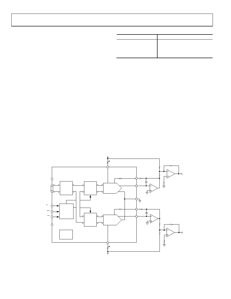
Bipolar Operation
In some applications, it may be necessary to generate full 4-quad-
rant multiplying operation or a bipolar output swing. This can
easily be accomplished by using another external amplifier and
some external resistors, as shown in Figure 39. In this circuit, the
second amplifier, A2, provides a gain of 2. Biasing the external
amplifier with an offset from the reference voltage results in full
4-quadrant multiplying operation. The transfer function of this
circuit shows that both negative and positive output voltages are
created as the input data (D) is incremented from Code 0 (VOUT =
VREF) to midscale (VOUT = 0 V) to full scale (VOUT = +VREF).
When connected in bipolar mode, the output voltage is given by
()
REF
n
REF
OUT
V
D
V
×
=
1
2
/
where:
D is the fractional representation of the digital word loaded to
the DAC.
D = 0 to 255 (AD5428)
= 0 to 1023 (AD5440)
= 0 to 4095 (AD5447)
n is the number of bits.
When VIN is an ac signal, the circuit performs 4-quadrant
multiplication. Table 8 shows the relationship between digital
code and the expected output voltage for bipolar operation
using the 8-bit AD5428.
Table 8. Bipolar Code
Digital Input
Analog Output (V)
1111 1111
+VREF (127/128)
1000 0000
0
0000 0001
–VREF (127/128)
0000 0000
–VREF (128/128)
Stability
In the I-to-V configuration, the IOUT of the DAC and the inverting
node of the op amp must be connected as close as possible, and
proper PCB layout techniques must be used. Because every code
change corresponds to a step function, gain peaking may occur
if the op amp has limited gain bandwidth product (GBP) and
there is excessive parasitic capacitance at the inverting node.
This parasitic capacitance introduces a pole into the open-loop
response, which can cause ringing or instability in the closed-
loop applications circuit.
An optional compensation capacitor, C1, can be added in parallel
small a value of C1 can produce ringing at the output, whereas
too large a value can adversely affect the settling time. C1 should
be found empirically, but 1 pF to 2 pF is generally adequate for
the compensation.
04462-031
CONTROL
LOGIC
INPUT
BUFFER
DATA
INPUTS
IOUTA
DB0
DAC A/B
CS
R/W
DGND
DB7
DB9
DB11
IOUTB
AGND
AD5428/AD5440/AD5447
LATCH
AGND
8-/10-/12-BIT
R-2R DAC A
8-/10-/12-BIT
R-2R DAC B
POWER-ON
RESET
VDD
VREFA
VINA
(±10V)
VREFB
RFBA
RFBB
R
RR21
VOUTA
R11
VINB
(±10V)
R31
R62
20k
Ω
R5
20k
Ω
R8
20k
Ω
R11
5k
Ω
R12
5k
Ω
R72
10k
Ω
R92
10k
Ω
R102
20k
Ω
C13
AGND
VOUTB
R41
C23
A1
A3
A2
A4
1R1, R2 AND R3, R4 USED ONLY IF GAIN ADJUSTMENT IS REQUIRED. ADJUST R1 FOR VOUTA = 0V WITH CODE 10000000 IN DAC A LATCH.
ADJUST R3 FOR VOUTB = 0V WITH CODE 10000000 IN DAC B LATCH.
2MATCHING AND TRACKING IS ESSENTIAL FOR RESISTOR PAIRS R6, R7 AND R9, R10.
3C1, C2 PHASE COMPENSATION (1pF TO 2pF) MAY BE REQUIRED IF A1/A3 IS A HIGH SPEED AMPLIFIER.
Figure 39. Bipolar Operation (4-Quadrant Multiplication)
相关PDF资料 |
PDF描述 |
|---|---|
| AD7801BRUZ-REEL | IC DAC 8BIT PARALLEL INP 20TSSOP |
| IDT5T9050PGGI | IC CLK BUFFER 1:5 200MHZ 28TSSOP |
| AD5312ARMZ-REEL7 | IC DAC 10BIT DUAL R-R 10-MSOP |
| VI-21W-MW-F3 | CONVERTER MOD DC/DC 5.5V 100W |
| IDT5V2310PGGI | IC CLK BUFF 1:10 200MHZ 24-TSSOP |
相关代理商/技术参数 |
参数描述 |
|---|---|
| AD5428YRUZ-REEL7 | 功能描述:IC DAC 8BIT MULTIPLYING 20TSSOP RoHS:是 类别:集成电路 (IC) >> 数据采集 - 数模转换器 系列:- 产品培训模块:Data Converter Fundamentals DAC Architectures 设计资源:Unipolar, Precision DC Digital-to-Analog Conversion using AD5450/1/2/3 8-14-Bit DACs (CN0052) Precision, Bipolar, Configuration for AD5450/1/2/3 8-14bit Multiplying DACs (CN0053) AC Signal Processing Using AD5450/1/2/3 Current Output DACs (CN0054) Programmable Gain Element Using AD5450/1/2/3 Current Output DAC Family (CN0055) Single Supply Low Noise LED Current Source Driver Using a Current Output DAC in the Reverse Mode (CN0139) 标准包装:10,000 系列:- 设置时间:- 位数:12 数据接口:DSP,MICROWIRE?,QSPI?,串行,SPI? 转换器数目:1 电压电源:单电源 功率耗散(最大):- 工作温度:-40°C ~ 125°C 安装类型:表面贴装 封装/外壳:SOT-23-8 薄型,TSOT-23-8 供应商设备封装:TSOT-23-8 包装:带卷 (TR) 输出数目和类型:1 电流,单极;1 电流,双极 采样率(每秒):2.7M |
| AD5429 | 制造商:AD 制造商全称:Analog Devices 功能描述:Dual 8-,10-,12-Bit High Bandwidth Multiplying DACs with Serial Interface |
| AD5429_13 | 制造商:AD 制造商全称:Analog Devices 功能描述:Dual 8-/10-/12-Bit, High Bandwidth, Multiplying DACs with Serial Interface |
| AD5429YRU | 功能描述:IC DAC DUAL 8BIT MULT 16-TSSOP RoHS:否 类别:集成电路 (IC) >> 数据采集 - 数模转换器 系列:- 产品培训模块:LTC263x 12-, 10-, and 8-Bit VOUT DAC Family 特色产品:LTC2636 - Octal 12-/10-/8-Bit SPI VOUT DACs with 10ppm/°C Reference 标准包装:91 系列:- 设置时间:4µs 位数:10 数据接口:MICROWIRE?,串行,SPI? 转换器数目:8 电压电源:单电源 功率耗散(最大):2.7mW 工作温度:-40°C ~ 85°C 安装类型:表面贴装 封装/外壳:14-WFDFN 裸露焊盘 供应商设备封装:14-DFN-EP(4x3) 包装:管件 输出数目和类型:8 电压,单极 采样率(每秒):* |
| AD5429YRU-REEL | 功能描述:IC DAC DUAL 8BIT MULT 16-TSSOP RoHS:否 类别:集成电路 (IC) >> 数据采集 - 数模转换器 系列:- 产品培训模块:Data Converter Fundamentals DAC Architectures 设计资源:Unipolar, Precision DC Digital-to-Analog Conversion using AD5450/1/2/3 8-14-Bit DACs (CN0052) Precision, Bipolar, Configuration for AD5450/1/2/3 8-14bit Multiplying DACs (CN0053) AC Signal Processing Using AD5450/1/2/3 Current Output DACs (CN0054) Programmable Gain Element Using AD5450/1/2/3 Current Output DAC Family (CN0055) Single Supply Low Noise LED Current Source Driver Using a Current Output DAC in the Reverse Mode (CN0139) 标准包装:10,000 系列:- 设置时间:- 位数:12 数据接口:DSP,MICROWIRE?,QSPI?,串行,SPI? 转换器数目:1 电压电源:单电源 功率耗散(最大):- 工作温度:-40°C ~ 125°C 安装类型:表面贴装 封装/外壳:SOT-23-8 薄型,TSOT-23-8 供应商设备封装:TSOT-23-8 包装:带卷 (TR) 输出数目和类型:1 电流,单极;1 电流,双极 采样率(每秒):2.7M |
发布紧急采购,3分钟左右您将得到回复。