- 您现在的位置:买卖IC网 > PDF目录8610 > AD5734RBREZ-REEL7 (Analog Devices Inc)IC DAC 14BIT DSP/SRL 24TSSOP PDF资料下载
参数资料
| 型号: | AD5734RBREZ-REEL7 |
| 厂商: | Analog Devices Inc |
| 文件页数: | 14/32页 |
| 文件大小: | 0K |
| 描述: | IC DAC 14BIT DSP/SRL 24TSSOP |
| 产品培训模块: | Data Converter Fundamentals DAC Architectures |
| 设计资源: | Software Configurable 14-Bit Quad-Channel Unipolar/Bipolar Voltage Output Using AD5734R (CN0084) |
| 标准包装: | 1,000 |
| 设置时间: | 10µs |
| 位数: | 14 |
| 数据接口: | DSP,MICROWIRE?,QSPI?,串行,SPI? |
| 转换器数目: | 4 |
| 电压电源: | 双 ± |
| 功率耗散(最大): | 310mW |
| 工作温度: | -40°C ~ 80°C |
| 安装类型: | 表面贴装 |
| 封装/外壳: | 24-TSSOP(0.173",4.40mm)裸露焊盘 |
| 供应商设备封装: | 24-TSSOP 裸露焊盘 |
| 包装: | 带卷 (TR) |
| 输出数目和类型: | 4 电压,单极;4 电压,双极 |
| 采样率(每秒): | 100k |
第1页第2页第3页第4页第5页第6页第7页第8页第9页第10页第11页第12页第13页当前第14页第15页第16页第17页第18页第19页第20页第21页第22页第23页第24页第25页第26页第27页第28页第29页第30页第31页第32页
AD5724R/AD5734R/AD5754R
Rev. E | Page 21 of 32
Standalone Operation
The serial interface works with both a continuous and a
noncontinuous serial clock. A continuous SCLK source can
only be used if SYNC is held low for the correct number of
clock cycles. In gated clock mode, a burst clock containing the
exact number of clock cycles must be used, and SYNC must be
taken high after the final clock to latch the data. The first falling
edge of SYNC starts the write cycle. Exactly 24 falling clock
edges must be applied to SCLK before SYNC is brought high
again. If SYNC is brought high before the 24th falling SCLK
edge, the data written is invalid. If more than 24 falling SCLK
edges are applied before SYNC is brought high, the input data
is also invalid. The input register addressed is updated on the
rising edge of SYNC. For another serial transfer to take place,
SYNC must be brought low again. After the end of the serial
data transfer, data is automatically transferred from the input
shift register to the addressed register.
When the data has been transferred into the chosen register
of the addressed DAC, all DAC registers and outputs can be
updated by taking LDAC low while SYNC is high.
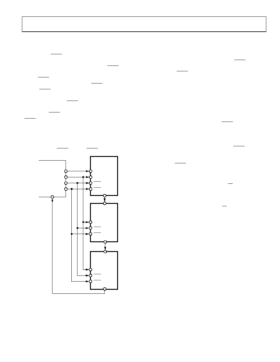
*ADDITIONAL PINS OMITTED FOR CLARITY.
68HC11*
MISO
SDIN
SCLK
MOSI
SCK
PC7
PC6
SDO
SCLK
SDO
SCLK
SDO
SDIN
SYNC
LDAC
AD5724R/
AD5734R/
AD5754R*
AD5724R/
AD5734R/
AD5754R*
AD5724R/
AD5734R/
AD5754R*
06
46
5-
0
08
Figure 46. Daisy Chaining the AD5724R/AD5734R/AD5754R
Daisy-Chain Operation
For systems that contain several devices, the SDO pin can be
used to daisy-chain several devices together. Daisy-chain mode
can be useful in system diagnostics and in reducing the number
of serial interface lines. The first falling edge of SYNC starts the
write cycle. SCLK is continuously applied to the input shift
register when SYNC is low. If more than 24 clock pulses are
applied, the data ripples out of the shift register and appears
on the SDO line. This data is clocked out on the rising edge of
SCLK and is valid on the falling edge. By connecting the SDO
of the first device to the SDIN input of the next device in the
chain, a multidevice interface is constructed. Each device in the
system requires 24 clock pulses. Therefore, the total number of
clock cycles must equal 24 × N, where N is the total number of
AD5724R/AD5734R/AD5754R devices in the chain. When the
serial transfer to all devices is complete, SYNC is taken high.
This latches the input data in each device in the daisy chain and
prevents any further data from being clocked into the input shift
register. The serial clock can be a continuous or gated clock.
A continuous SCLK source can only be used if SYNC is held
low for the correct number of clock cycles. In gated clock mode,
a burst clock containing the exact number of clock cycles must
be used, and SYNC must be taken high after the final clock to
latch the data.
Readback Operation
Readback mode is invoked by setting the R/W bit to 1 in the
write operation to the serial input shift register. (If the SDO
output is disabled via the SDO disable bit in the control register,
it is automatically enabled for the duration of the read operation,
after which it is disabled again.) With R/W set to 1, Bit A2 to Bit
A0 in association with Bit REG2 to Bit REG0 select the register
to be read. The remaining data bits in the write sequence are don’t
care bits. During the next SPI write, the data appearing on the
SDO output contains the data from the previously addressed
register. For a read of a single register, the NOP command can
be used in clocking out the data from the selected register on
SDO. The readback diagram in
shows the readback
sequence. For example, to read back the DAC register of
Channel A, the following sequence should be implemented:
1.
Write 0x800000 to the AD5724R/AD5734R/AD5754R
input register. This configures the part for read mode
with the DAC register of Channel A selected. Note that
all the data bits, DB15 to DB0, are don’t care bits.
2.
Follow this with a second write, a NOP condition, 0x180000.
During this write, the data from the register is clocked out
on the SDO line.
相关PDF资料 |
PDF描述 |
|---|---|
| AD8138ARM-REEL7 | IC AMP DIFF LDIST LP 95MA 8MSOP |
| AD8138AR-REEL7 | IC AMP DIFF LDIST LP 95MA 8SOIC |
| LTC2610IUFD#TRPBF | IC DAC OCTAL R-R 14BIT 20-QFN |
| AD8310ARMZ-REEL7 | IC AMP LOGARITHMIC 8MSOP |
| VE-24P-IV-F1 | CONVERTER MOD DC/DC 13.8V 150W |
相关代理商/技术参数 |
参数描述 |
|---|---|
| AD5735 | 制造商:AD 制造商全称:Analog Devices 功能描述:Quad Channel, 16-Bit, Serial Input, 4-20mA & Voltage Output DAC, Dynamic Power Control |
| AD5735_12 | 制造商:AD 制造商全称:Analog Devices 功能描述:Quad-Channel, 12-Bit, Serial Input, 4 mA to 20 mA |
| AD5735ACPZ | 功能描述:IC DAC QUAD VOLT CUR 64-LFCSP RoHS:是 类别:集成电路 (IC) >> 数据采集 - 数模转换器 系列:- 标准包装:1 系列:- 设置时间:4.5µs 位数:12 数据接口:串行,SPI? 转换器数目:1 电压电源:单电源 功率耗散(最大):- 工作温度:-40°C ~ 125°C 安装类型:表面贴装 封装/外壳:8-SOIC(0.154",3.90mm 宽) 供应商设备封装:8-SOICN 包装:剪切带 (CT) 输出数目和类型:1 电压,单极;1 电压,双极 采样率(每秒):* 其它名称:MCP4921T-E/SNCTMCP4921T-E/SNRCTMCP4921T-E/SNRCT-ND |
| AD5735ACPZ-REEL7 | 功能描述:IC DAC QUAD VOLT CUR 64LFCSP RoHS:是 类别:集成电路 (IC) >> 数据采集 - 数模转换器 系列:- 产品培训模块:Data Converter Fundamentals DAC Architectures 标准包装:750 系列:- 设置时间:7µs 位数:16 数据接口:并联 转换器数目:1 电压电源:双 ± 功率耗散(最大):100mW 工作温度:0°C ~ 70°C 安装类型:表面贴装 封装/外壳:28-LCC(J 形引线) 供应商设备封装:28-PLCC(11.51x11.51) 包装:带卷 (TR) 输出数目和类型:1 电压,单极;1 电压,双极 采样率(每秒):143k |
| AD5737 | 制造商:AD 制造商全称:Analog Devices 功能描述:Quad Channel, 16-Bit, Serial Input, 4-20mA Output DAC, Dynamic Power Control, HART Connectivity |
发布紧急采购,3分钟左右您将得到回复。