参数资料
| 型号: | AD5781BRUZ-REEL7 |
| 厂商: | Analog Devices Inc |
| 文件页数: | 15/28页 |
| 文件大小: | 0K |
| 描述: | IC DAC 18BIT SRL 20TSSOP |
| 产品变化通告: | AD57x1 Feature Change 27/Jul/2011 |
| 设计资源: | 18-Bit Accurate, low noise, precision bipolar DC voltage source (CN0177) |
| 标准包装: | 1,000 |
| 设置时间: | 1µs |
| 位数: | 18 |
| 数据接口: | DSP,MICROWIRE?,QSPI?,串行,SPI? |
| 转换器数目: | 1 |
| 电压电源: | 模拟和数字,双 ± |
| 工作温度: | -40°C ~ 125°C |
| 安装类型: | 表面贴装 |
| 封装/外壳: | 20-TSSOP(0.173",4.40mm 宽) |
| 供应商设备封装: | 20-TSSOP |
| 包装: | 带卷 (TR) |
| 输出数目和类型: | * |
| 采样率(每秒): | 1M |
第1页第2页第3页第4页第5页第6页第7页第8页第9页第10页第11页第12页第13页第14页当前第15页第16页第17页第18页第19页第20页第21页第22页第23页第24页第25页第26页第27页第28页
AD5781
Data Sheet
Rev. D | Page 22 of 28
Control Register
The control register controls the mode of operation of the AD5781.
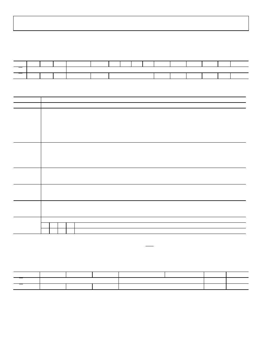
Table 11. Control Register
MSB
LSB
DB23
DB22
DB21
DB20
DB19...DB11
DB10
DB9
DB8
DB7
DB6
DB5
DB4
DB3
DB2
DB1
DB0
R/
W
Register address
Control register data
R/
W
0
1
0
Reserved
LIN COMP
SDODIS
BIN/2sC
DACTRI
OPGND
RBUF
Reserved
Table 12. Control Register Functions
Clearcode Register
The clearcode register sets the value to which the DAC output is set when the CLR pin or CLR bit is asserted. The output value depends
on the DAC coding that is being used, either binary or twos complement. The default register value is 0.
Table 13. Clearcode Register
MSB
LSB
DB23
DB22
DB21
DB20
DB19
DB2
DB1
DB0
R/W
Register address
Clearcode register data
R/W
0
1
18-bits of data
X1
1
X is don’t care.
Function
Description
Reserved
These bits are reserved and should be programmed to zero.
RBUF
Output amplifier configuration control.
0: internal amplifier, A1, is powered up and resistors RFB and R1 are connected in series as shown in Figure 52. This allows
an external amplifier to be connected in a gain of two configurations. See the AD5781 Features section for further details.
1: (default) internal amplifier, A1, is powered down and resistors RFB and R1 are connected in parallel as shown in Figure 51
so that the resistance between the RFB and INV pins is 3.4 k, equal to the resistance of the DAC. This allows the RFB and INV
pins to be used for input bias current compensation for an external unity gain amplifier. See the AD5781 Features section
for further details.
OPGND
Output ground clamp control.
0: DAC output clamp to ground is removed, and the DAC is placed in normal mode.
1: (default) DAC output is clamped to ground through a ~6 k resistance, and the DAC is placed in tristate mode.
Resetting the part puts the DAC in OPGND mode, where the output ground clamp is enabled and the DAC is tristated.
Setting the OPGND bit to 1 in the control register overrules any write to the DACTRI bit
DACTRI
DAC tristate control.
0: DAC is in normal operating mode.
1: (default) DAC is in tristate mode.
BIN/2sC
DAC register coding select.
0: (default) DAC register uses twos complement coding.
1: DAC register uses offset binary coding.
SDODIS
SDO pin enable/disable control.
0: (default) SDO pin is enabled.
1: SDO pin is disabled (tristate).
LIN COMP
Linearity error compensation for varying reference input spans. See the AD5781 Features section for further details.
0
(Default) reference input span up to 10 V.
1
0
Reference input span of 20 V.
相关PDF资料 |
PDF描述 |
|---|---|
| AD5790BCPZ | IC DAC VOLT OUT 20BIT 24LFCSP |
| AD5791BRUZ | IC DAC 20BIT SRL 20TSSOP |
| AD5821ABCBZ-REEL | IC DAC 10BIT CURRENTSINK 9WLCSP |
| AD6600ASTZ | IC ADC DUAL W/RSSI 44-LQFP |
| AD6644ASTZ-65 | IC ADC 14BIT 65MSPS CMOS 52-LQFP |
相关代理商/技术参数 |
参数描述 |
|---|---|
| AD5781SRU-EP | 功能描述:数模转换器- DAC 18-Bit VOut +/-0.5 LSB INL RoHS:否 制造商:Analog Devices 转换器数量:4 DAC 输出端数量:4 转换速率: 分辨率:12 bit 接口类型:Serial (I2C) 稳定时间: 最大工作温度:+ 105 C 安装风格: 封装 / 箱体:TSSOP 封装:Reel |
| AD578221 | 制造商: 功能描述: 制造商:undefined 功能描述: |
| AD578JD | 制造商:AD 制造商全称:Analog Devices 功能描述:VERY FAST, COMPLETE 10- OR 12-BIT A/D CONVERTERS |
| AD578JN | 制造商:AD 制造商全称:Analog Devices 功能描述:VERY FAST, COMPLETE 10- OR 12-BIT A/D CONVERTERS |
| AD578K | 制造商:AD 制造商全称:Analog Devices 功能描述:VERY FAST, COMPLETE 10- OR 12-BIT A/D CONVERTERS |
发布紧急采购,3分钟左右您将得到回复。