参数资料
| 型号: | AD5781BRUZ-REEL7 |
| 厂商: | Analog Devices Inc |
| 文件页数: | 27/28页 |
| 文件大小: | 0K |
| 描述: | IC DAC 18BIT SRL 20TSSOP |
| 产品变化通告: | AD57x1 Feature Change 27/Jul/2011 |
| 设计资源: | 18-Bit Accurate, low noise, precision bipolar DC voltage source (CN0177) |
| 标准包装: | 1,000 |
| 设置时间: | 1µs |
| 位数: | 18 |
| 数据接口: | DSP,MICROWIRE?,QSPI?,串行,SPI? |
| 转换器数目: | 1 |
| 电压电源: | 模拟和数字,双 ± |
| 工作温度: | -40°C ~ 125°C |
| 安装类型: | 表面贴装 |
| 封装/外壳: | 20-TSSOP(0.173",4.40mm 宽) |
| 供应商设备封装: | 20-TSSOP |
| 包装: | 带卷 (TR) |
| 输出数目和类型: | * |
| 采样率(每秒): | 1M |
第1页第2页第3页第4页第5页第6页第7页第8页第9页第10页第11页第12页第13页第14页第15页第16页第17页第18页第19页第20页第21页第22页第23页第24页第25页第26页当前第27页第28页
AD5781
Data Sheet
Rev. D | Page 8 of 28
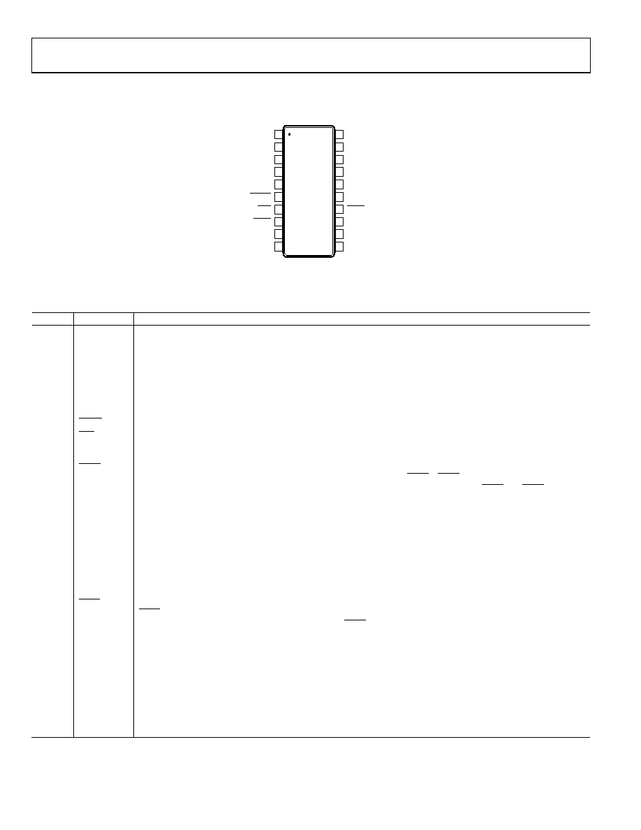
PIN CONFIGURATION AND FUNCTION DESCRIPTION
1
2
3
4
5
6
7
8
9
10
VOUT
VREFPS
VREFPF
CLR
RESET
VDD
INV
IOVCC
VCC
LDAC
20
19
18
17
16
15
14
13
12
11
AGND
VSS
VREFNS
SYNC
DGND
VREFNF
SDO
SDIN
SCLK
RFB
AD5781
TOP VIEW
(Not to Scale)
09092-
005
Figure 4. Pin Configuration
Table 6. Pin Function Descriptions
Pin No.
Mnemonic
Description
1
INV
Connection to Inverting Input of External Amplifier. See the AD5781 Features section for further details.
2
VOUT
Analog Output Voltage.
3
VREFPS
Positive Reference Sense Voltage Input. A voltage range of 5 V to VDD 2.5 V can be connected. A unity gain amplifier
must be connected at this pin, in conjunction with the VREFPF pin. See the AD5781 Features section for further details.
4
VREFPF
Positive Reference Force Voltage Input. A voltage range of 5 V to VDD 2.5 V can be connected. A unity gain amplifier
must be connected at these pin, in conjunction with the VREFPS pin. See AD5781 Features section for further details.
5
VDD
Positive Analog Supply Connection. A voltage range of 7.5 V to 16.5 V can be connected. VDD should be decoupled to
AGND.
6
RESET
Active Low Reset Logic Input Pin. Asserting this pin returns the AD5781 to its power-on status.
7
CLR
Active Low Clear Logic Input Pin. Asserting this pin sets the DAC register to a user defined value (see Table 13) and
updates the DAC output. The output value depends on the DAC register coding that is being used, either binary or twos
complement.
8
LDAC
Active Low Load DAC Logic Input Pin. This is used to update the DAC register and, consequently, the analog output.
When tied permanently low, the output is updated on the rising edge of SYNC. If LDAC is held high during the write
cycle, the input register is updated, but the output update is held off until the falling edge of LDAC. The LDAC pin
should not be left unconnected.
9
VCC
Digital Supply Connection. A voltage in the range of 2.7 V to 5.5 V can be connected. VCC should be decoupled to DGND.
10
IOVCC
Digital Interface Supply Pin. Digital threshold levels are referenced to the voltage applied to this pin. A voltage range of
1.71 V to 5.5 V can be connected. IOVCC should not be allowed to exceed VCC.
11
SDO
Serial Data Output Pin. Data is clocked out on the rising edge of the serial clock input.
12
SDIN
Serial Data Input Pin. This device has a 24-bit shift register. Data is clocked into the register on the falling edge of the
serial clock input.
13
SCLK
Serial Clock Input. Data is clocked into the input shift register on the falling edge of the serial clock input. Data can be
transferred at clock rates of up to 35 MHz.
14
SYNC
Active Low Digital Interface Synchronization Input Pin. This is the frame synchronization signal for the input data. When
SYNC is low, it enables the input shift register, and data is then transferred in on the falling edges of the following clocks.
The input shift register is updated on the rising edge of SYNC.
15
DGND
Ground Reference Pin for Digital Circuitry.
16
VREFNF
Negative Reference Force Voltage Input. A voltage range of VSS + 2.5 V to 0 V can be connected. A unity gain amplifier
must be connected at this pin, in conjunction with the VREFNS pin. See the AD5781 Features section for further details.
17
VREFNS
Negative Reference Sense Voltage Input. A voltage range of VSS + 2.5 V to 0 V can be connected. A unity gain amplifier
must be connected at these pin, in conjunction with the VREFNF pin. See the AD5781 Features section for further details.
18
VSS
Negative Analog Supply Connection. A voltage range of 16.5 V to 2.5 V can be connected. VSS should be decoupled to
AGND.
19
AGND
Ground Reference Pin for Analog Circuitry.
20
RFB
Feedback Connection for External Amplifier. See the AD5781 Features section for further details.
相关PDF资料 |
PDF描述 |
|---|---|
| AD5790BCPZ | IC DAC VOLT OUT 20BIT 24LFCSP |
| AD5791BRUZ | IC DAC 20BIT SRL 20TSSOP |
| AD5821ABCBZ-REEL | IC DAC 10BIT CURRENTSINK 9WLCSP |
| AD6600ASTZ | IC ADC DUAL W/RSSI 44-LQFP |
| AD6644ASTZ-65 | IC ADC 14BIT 65MSPS CMOS 52-LQFP |
相关代理商/技术参数 |
参数描述 |
|---|---|
| AD5781SRU-EP | 功能描述:数模转换器- DAC 18-Bit VOut +/-0.5 LSB INL RoHS:否 制造商:Analog Devices 转换器数量:4 DAC 输出端数量:4 转换速率: 分辨率:12 bit 接口类型:Serial (I2C) 稳定时间: 最大工作温度:+ 105 C 安装风格: 封装 / 箱体:TSSOP 封装:Reel |
| AD578221 | 制造商: 功能描述: 制造商:undefined 功能描述: |
| AD578JD | 制造商:AD 制造商全称:Analog Devices 功能描述:VERY FAST, COMPLETE 10- OR 12-BIT A/D CONVERTERS |
| AD578JN | 制造商:AD 制造商全称:Analog Devices 功能描述:VERY FAST, COMPLETE 10- OR 12-BIT A/D CONVERTERS |
| AD578K | 制造商:AD 制造商全称:Analog Devices 功能描述:VERY FAST, COMPLETE 10- OR 12-BIT A/D CONVERTERS |
发布紧急采购,3分钟左右您将得到回复。