参数资料
| 型号: | AD603ARZ-REEL |
| 厂商: | Analog Devices Inc |
| 文件页数: | 10/25页 |
| 文件大小: | 0K |
| 描述: | IC AMP VGA 90MHZ LN 50MA 8SOIC |
| 标准包装: | 2,500 |
| 系列: | X-AMP® |
| 放大器类型: | 可变增益 |
| 电路数: | 1 |
| 转换速率: | 275 V/µs |
| -3db带宽: | 90MHz |
| 电流 - 输入偏压: | 200nA |
| 电流 - 电源: | 12.5mA |
| 电流 - 输出 / 通道: | 50mA |
| 电压 - 电源,单路/双路(±): | 9.5 V ~ 12.6 V,±4.75 V ~ 6.3 V |
| 工作温度: | -40°C ~ 85°C |
| 安装类型: | 表面贴装 |
| 封装/外壳: | 8-SOIC(0.154",3.90mm 宽) |
| 供应商设备封装: | 8-SO |
| 包装: | 带卷 (TR) |
| 配用: | AD603-EVALZ-ND - BOARD EVALUATION FOR AD603 |
Data Sheet
AD603
Rev. K | Page 17 of 24
connected to the control voltage and the GNEW inputs are
grounded. The gain scaling is then doubled to 80 dB/V,
requiring only a 1.00 V change for an 80 dB change of gain
Gain = (dB) = 80 VG + GO
(4)
where, as before, GO depends on the range selected; for example,
in the maximum bandwidth mode, GO is 20 dB. Alternatively,
the GNEG pins may be connected to an offset voltage of
0.500 V, in which case GO is 20 dB.
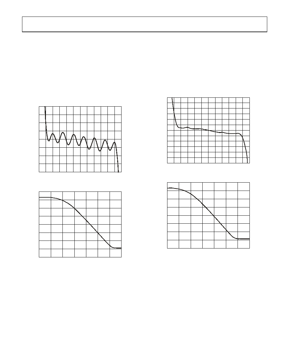
The amplitude of the gain ripple in this case is also doubled, as
shown in Figure 45, while the ISNR at the output of A2 now
decreases linearly as the gain increases, as shown in Figure 46.
00539-
043
VC (V)
2.2
–0.2
0
0.2
0.4
0.6
1.0
1.2
0.8
1.6
1.8
2.0
1.4
G
AI
N
E
RRO
R
(
d
B)
2.0
1.5
1.0
0.5
0
–0.5
–1.0
–1.5
–2.0
Figure 45. Gain Error for Cascaded Stages—Parallel Control
00539-
044
VC (V)
1.2
–0.2
0
0.2
0.4
0.6
0.8
1.0
IS
NR
(
d
B)
90
80
85
75
65
70
55
60
50
Figure 46. ISNR for Cascaded Stages—Parallel Control
LOW GAIN RIPPLE MODE (MINIMUM GAIN ERROR)
As can be seen in Figure 44 and Figure 45, the error in the gain
is periodic, that is, it shows a small ripple. (Note that there is
also a variation in the output offset voltage, which is due to the
gain interpolation, but this is not exact in amplitude.) By
offsetting the gains of A1 and A2 by half the period of the ripple,
that is, by 3 dB, the residual gain errors of the two amplifiers
can be made to cancel. Figure 47 shows much lower gain ripple
when configured in this manner. Figure 48 plots the ISNR as a
function of gain; it is very similar to that in the parallel mode.
00539-
045
VC (V)
1.1
–0.1
0
0.1
0.2
0.3
0.4
0.5
0.6
0.7
0.8
0.9
1.0
G
AI
N
E
RRO
R
(
d
B)
3.0
2.5
2.0
1.5
1.0
0.5
–0.5
–1.0
0
–1.5
–2.0
–2.5
–3.0
Figure 47. Gain Error for Cascaded Stages—Low Ripple Mode
00539-
046
VC (V)
1.2
–0.2
0
0.2
0.4
0.6
0.8
1.0
IS
NR
(
d
B)
90
85
80
75
70
65
60
55
50
Figure 48. ISNR vs. Control Voltage—Low Ripple Mode
相关PDF资料 |
PDF描述 |
|---|---|
| AD5750BCPZ | IC CURR/VOLT OUT DVR 32LFCSP |
| SM6S20AHE3/2D | TVS 6W 20V 5% SMD DO-218AB |
| SM6S18AHE3/2D | TVS 6W 18V 5% SMD DO-218AB |
| SM6S17AHE3/2D | TVS 6W 17V 5% SMD DO-218AB |
| SM6S16AHE3/2D | TVS 6W 16V 5% SMD DO-218AB |
相关代理商/技术参数 |
参数描述 |
|---|---|
| AD603ARZ-REEL7 | 功能描述:IC AMP VGA 90MHZ LN 50MA 8SOIC RoHS:是 类别:集成电路 (IC) >> Linear - Amplifiers - Instrumentation 系列:X-AMP® 标准包装:150 系列:- 放大器类型:音频 电路数:2 输出类型:- 转换速率:5 V/µs 增益带宽积:12MHz -3db带宽:- 电流 - 输入偏压:100nA 电压 - 输入偏移:500µV 电流 - 电源:6mA 电流 - 输出 / 通道:50mA 电压 - 电源,单路/双路(±):4 V ~ 32 V,±2 V ~ 16 V 工作温度:-40°C ~ 85°C 安装类型:表面贴装 封装/外壳:8-TSSOP(0.173",4.40mm 宽) 供应商设备封装:8-TSSOP 包装:管件 |
| AD603-EB | 制造商:Analog Devices 功能描述:Evaluation Board For Low Noise, 90 MHz Variable Gain Amplifier |
| AD603-EVALZ | 功能描述:BOARD EVALUATION FOR AD603 RoHS:是 类别:编程器,开发系统 >> 评估板 - 运算放大器 系列:X-AMP® 产品培训模块:Lead (SnPb) Finish for COTS Obsolescence Mitigation Program 标准包装:1 系列:- |
| AD603SQ/883B | 功能描述:差分放大器 IC 90 MHz VARIABLE GAIN AMP RoHS:否 制造商:Analog Devices 通道数量:1 Channel 带宽:900 MHz 可用增益调整:5.6 dB to 20 dB 输入补偿电压:1 mV at 5 V 共模抑制比(最小值):67 dB 工作电源电压:11 V 电源电流:28 mA 最大工作温度:+ 85 C 最小工作温度:- 40 C 安装风格:SMD/SMT 封装 / 箱体:SOIC-8 封装:Reel |
| AD603SQ/883B2 | 制造商:AD 制造商全称:Analog Devices 功能描述:Low Noise, 90 MHz Variable Gain Amplifier |
发布紧急采购,3分钟左右您将得到回复。