参数资料
| 型号: | AD603ARZ-REEL |
| 厂商: | Analog Devices Inc |
| 文件页数: | 6/25页 |
| 文件大小: | 0K |
| 描述: | IC AMP VGA 90MHZ LN 50MA 8SOIC |
| 标准包装: | 2,500 |
| 系列: | X-AMP® |
| 放大器类型: | 可变增益 |
| 电路数: | 1 |
| 转换速率: | 275 V/µs |
| -3db带宽: | 90MHz |
| 电流 - 输入偏压: | 200nA |
| 电流 - 电源: | 12.5mA |
| 电流 - 输出 / 通道: | 50mA |
| 电压 - 电源,单路/双路(±): | 9.5 V ~ 12.6 V,±4.75 V ~ 6.3 V |
| 工作温度: | -40°C ~ 85°C |
| 安装类型: | 表面贴装 |
| 封装/外壳: | 8-SOIC(0.154",3.90mm 宽) |
| 供应商设备封装: | 8-SO |
| 包装: | 带卷 (TR) |
| 配用: | AD603-EVALZ-ND - BOARD EVALUATION FOR AD603 |
Data Sheet
AD603
Rev. K | Page 13 of 24
SCALING
REFERENCE
VG
GAIN-
CONTROL
INTERFACE
AD603
PRECISION PASSIVE
INPUT ATTENUATOR
FIXED-GAIN
AMPLIFIER
*NOMINAL VALUES.
R-2R LADDER NETWORK
VPOS
VNEG
GPOS
GNEG
VINP
COMM
0dB
–6.02dB –12.04dB –18.06dB –24.08dB –30.1dB –36.12dB –42.14dB
R
RR
RRR
R
2R
R
20*
694*
6.44k*
VOUT
FDBK
00
53
9-
0
29
8
6
1
2
5
7
4
3
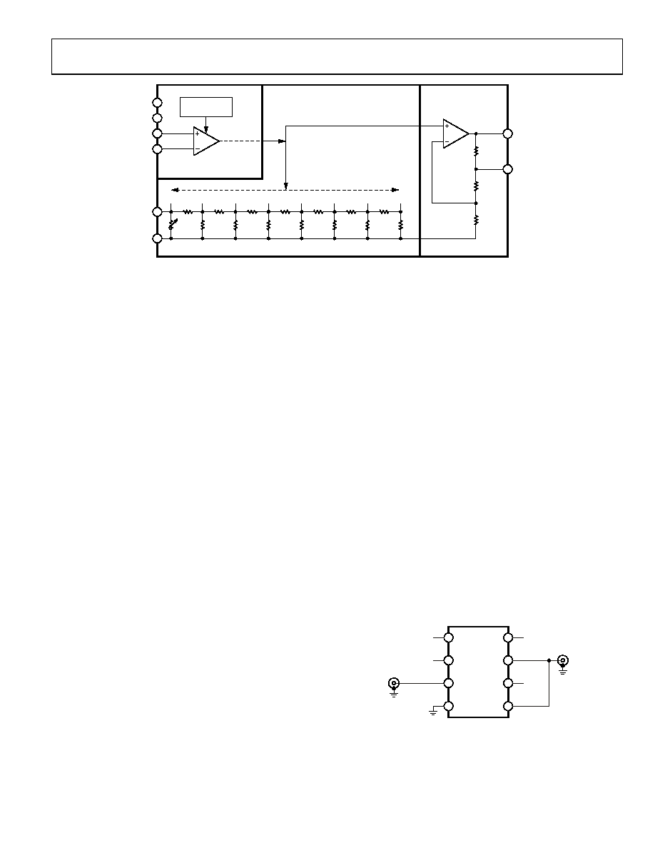
Figure 31. Simplified Block Diagram
THE GAIN CONTROL INTERFACE
The attenuation is controlled through a differential, high
impedance (50 MΩ) input, with a scaling factor that is laser-
trimmed to 40 dB per volt, that is, 25 mV/dB. An internal band
gap reference ensures stability of the scaling with respect to
supply and temperature variations.
When the differential input voltage VG = 0 V, the attenuator
slider is centered, providing an attenuation of 21.07 dB. For the
maximum bandwidth range, this results in an overall gain of
10 dB (= 21.07 dB + 31.07 dB). When the control input is
500 mV, the gain is lowered by +20 dB (= 0.500 V × 40 dB/V)
to 10 dB; when set to +500 mV, the gain is increased by
+20 dB to +30 dB. When this interface is overdriven in either
direction, the gain approaches either 11.07 dB (= 42.14 dB +
+31.07 dB) or 31.07 dB (= 0 + 31.07 dB), respectively. The only
constraint on the gain control voltage is that it be kept within
the common-mode range (1.2 V to +2.0 V assuming +5 V
supplies) of the gain control interface.
The basic gain of the AD603 can therefore be calculated by
Gain (dB) = 40 VG +10
(1)
where VG is in volts. When Pin 5 and Pin 7 are strapped (see the
section), the gain becomes
Gain (dB) = 40 VG + 20 for 0 to +40 dB
and
Gain (dB) = 40 VG + 30 for +10 to +50 dB
(2)
The high impedance gain control input ensures minimal
loading when driving many amplifiers in multiple channel
or cascaded applications. The differential capability provides
flexibility in choosing the appropriate signal levels and
polarities for various control schemes.
For example, if the gain is to be controlled by a DAC providing
a positive-only, ground-referenced output, the gain control low
(GNEG) pin should be biased to a fixed offset of 500 mV to set
the gain to 10 dB when gain control high (GPOS) is at zero,
and to 30 dB when at 1.00 V.
It is a simple matter to include a voltage divider to achieve other
scaling factors. When using an 8-bit DAC having an FS output
of 2.55 V (10 mV/bit), a divider ratio of 2 (generating 5 mV/bit)
results in a gain-setting resolution of 0.2 dB/bit. The use of such
offsets is valuable when two AD603s are cascaded, when
various options exist for optimizing the signal-to-noise profile,
as is shown in the Sequential Mode (Optimal SNR) section,
PROGRAMMING THE FIXED-GAIN AMPLIFIER
USING PIN STRAPPING
Access to the feedback network is provided at Pin 5 (FDBK).
The user may program the gain of the output amplifier of the
AD603 using this pin, as shown in Figure 32, Figure 33, and
Figure 34. There are three modes: in the default mode, FDBK
is unconnected, providing the range +9 dB/+51 dB; when VOUT
and FDBK are shorted, the gain is lowered to 11 dB/+31 dB;
and, when an external resistor is placed between VOUT and
FDBK, any intermediate gain can be achieved, for example,
1 dB/+41 dB. Figure 35 shows the nominal maximum gain vs.
external resistor for this mode.
GPOS
GNEG
VINP
COMM
VPOS
VOUT
VNEG
FDBK
AD603
VC1
VC2
VIN
VPOS
VOUT
VNEG
00
53
9-
0
30
8
7
6
5
1
2
3
4
Figure 32. 10 dB to +30 dB; 90 MHz Bandwidth
相关PDF资料 |
PDF描述 |
|---|---|
| AD5750BCPZ | IC CURR/VOLT OUT DVR 32LFCSP |
| SM6S20AHE3/2D | TVS 6W 20V 5% SMD DO-218AB |
| SM6S18AHE3/2D | TVS 6W 18V 5% SMD DO-218AB |
| SM6S17AHE3/2D | TVS 6W 17V 5% SMD DO-218AB |
| SM6S16AHE3/2D | TVS 6W 16V 5% SMD DO-218AB |
相关代理商/技术参数 |
参数描述 |
|---|---|
| AD603ARZ-REEL7 | 功能描述:IC AMP VGA 90MHZ LN 50MA 8SOIC RoHS:是 类别:集成电路 (IC) >> Linear - Amplifiers - Instrumentation 系列:X-AMP® 标准包装:150 系列:- 放大器类型:音频 电路数:2 输出类型:- 转换速率:5 V/µs 增益带宽积:12MHz -3db带宽:- 电流 - 输入偏压:100nA 电压 - 输入偏移:500µV 电流 - 电源:6mA 电流 - 输出 / 通道:50mA 电压 - 电源,单路/双路(±):4 V ~ 32 V,±2 V ~ 16 V 工作温度:-40°C ~ 85°C 安装类型:表面贴装 封装/外壳:8-TSSOP(0.173",4.40mm 宽) 供应商设备封装:8-TSSOP 包装:管件 |
| AD603-EB | 制造商:Analog Devices 功能描述:Evaluation Board For Low Noise, 90 MHz Variable Gain Amplifier |
| AD603-EVALZ | 功能描述:BOARD EVALUATION FOR AD603 RoHS:是 类别:编程器,开发系统 >> 评估板 - 运算放大器 系列:X-AMP® 产品培训模块:Lead (SnPb) Finish for COTS Obsolescence Mitigation Program 标准包装:1 系列:- |
| AD603SQ/883B | 功能描述:差分放大器 IC 90 MHz VARIABLE GAIN AMP RoHS:否 制造商:Analog Devices 通道数量:1 Channel 带宽:900 MHz 可用增益调整:5.6 dB to 20 dB 输入补偿电压:1 mV at 5 V 共模抑制比(最小值):67 dB 工作电源电压:11 V 电源电流:28 mA 最大工作温度:+ 85 C 最小工作温度:- 40 C 安装风格:SMD/SMT 封装 / 箱体:SOIC-8 封装:Reel |
| AD603SQ/883B2 | 制造商:AD 制造商全称:Analog Devices 功能描述:Low Noise, 90 MHz Variable Gain Amplifier |
发布紧急采购,3分钟左右您将得到回复。