参数资料
| 型号: | AD603ARZ-REEL |
| 厂商: | Analog Devices Inc |
| 文件页数: | 9/25页 |
| 文件大小: | 0K |
| 描述: | IC AMP VGA 90MHZ LN 50MA 8SOIC |
| 标准包装: | 2,500 |
| 系列: | X-AMP® |
| 放大器类型: | 可变增益 |
| 电路数: | 1 |
| 转换速率: | 275 V/µs |
| -3db带宽: | 90MHz |
| 电流 - 输入偏压: | 200nA |
| 电流 - 电源: | 12.5mA |
| 电流 - 输出 / 通道: | 50mA |
| 电压 - 电源,单路/双路(±): | 9.5 V ~ 12.6 V,±4.75 V ~ 6.3 V |
| 工作温度: | -40°C ~ 85°C |
| 安装类型: | 表面贴装 |
| 封装/外壳: | 8-SOIC(0.154",3.90mm 宽) |
| 供应商设备封装: | 8-SO |
| 包装: | 带卷 (TR) |
| 配用: | AD603-EVALZ-ND - BOARD EVALUATION FOR AD603 |
AD603
Data Sheet
Rev. K | Page 16 of 24
The gains are offset (Figure 41) such that the gain of A2 is
increased only after the gain of A1 has reached its maximum
value. Note that for a differential input of –600 mV or less, the
gain of a single amplifier (A1 or A2) is at its minimum value of
11.07 dB; for a differential input of 600 mV or more, the gain
is at its maximum value of 31.07 dB. Control inputs beyond
these limits do not affect the gain and can be tolerated without
damage or foldover in the response. This is an important aspect
of the gain control response of the AD603. (See the Specifications
section for more details on the allowable voltage range.) The
gain is now
Gain (dB) = 40 VG + GO
(3)
where:
VG is the applied control voltage.
GO is determined by the gain range chosen.
In the explanatory notes that follow, it is assumed that
the maximum bandwidth connections are used, for which
GO is 20 dB.
+31.07dB
+10dB
A1
A2
+31.07dB
+28.96dB
–11.07dB
0.473
1.526
–8.93dB
0
–20
0.5
0
1.0
20
1.50
40
2.0
60
VC (V)
62.14
–22.14
GAIN
(dB)
*GAIN OFFSET OF 1.07dB, OR 26.75mV.
00
53
9-
0
39
*
Figure 41. Explanation of Offset Calibration for Sequential Control
With reference to Figure 38, Figure 39, and Figure 40, note that
VG1 refers to the differential gain control input to A1, and VG2
refers to the differential gain control input to A2. When VG is
0 V, VG1 = 473 mV and thus the gain of A1 is 8.93 dB (recall
that the gain of each individual amplifier in the maximum
bandwidth mode is –10 dB for VG = 500 mV and 10 dB for VG
= 0 V); meanwhile, VG2 = 1.908 V so the gain of A2 is pinned
at 11.07 dB. The overall gain is therefore –20 dB (see Figure 38).
When VG = 1.00 V, VG1 = 1.00 V 0.473 V = 0.526 V, which sets
the gain of A1 to nearly its maximum value of +31.07 dB, while
VG2 = 1.00 V 1.526 V = 0.526 V, which sets the gain of A2 to
nearly its minimum value of 11.07 dB. Close analysis shows
that the degree to which neither AD603 is completely pushed to
its maximum nor minimum gain exactly cancels in the overall
gain, which is now 20 dB (see Figure 39).
When VG = 2.0 V, the gain of A1 is pinned at 31.07 dB and that
of A2 is near its maximum value of 28.93 dB, resulting in an
overall gain of 60 dB (see Figure 40). This mode of operation is
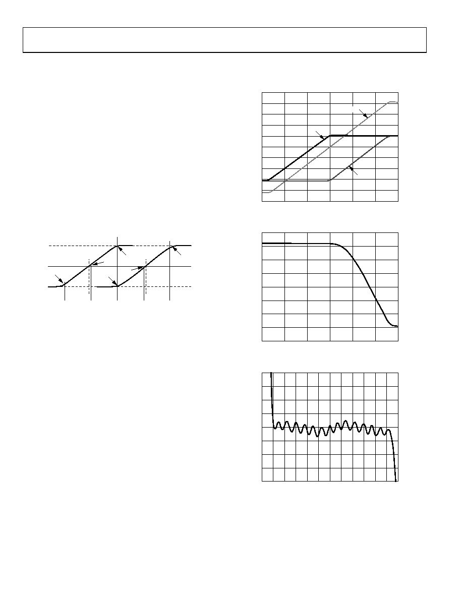
further clarified in Figure 42, which is a plot of the separate
gains of A1 and A2 and the overall gain vs. the control voltage.
Figure 43 is a plot of the SNR of the cascaded amplifiers vs. the
control voltage. Figure 44 is a plot of the gain error of the
cascaded stages vs. the control voltages.
00
53
9-
0
4
0
VC (V)
2.0
–0.2
0.2
0.6
1.0
1.4
1.8
OV
E
R
A
L
G
A
IN
(
d
B
)
70
50
60
40
30
20
10
0
–10
–20
–30
COMBINED
A1
A2
Figure 42. Plot of Separate and Overall Gains in Sequential Control
00
53
9-
0
4
1
VC (V)
2.0
–0.2
0.2
0.6
1.0
1.4
1.8
S
NR
(
d
B)
90
80
70
60
50
40
30
20
10
Figure 43. SNR for Cascaded Stages—Sequential Control
00
53
9-
0
4
2
VC (V)
2.2
–0.2
0
0.2 0.4 0.6 0.8 1.0 1.2 1.4 1.6 1.8 2.0
G
AI
N
E
R
RO
R
(
d
B)
2.0
1.5
1.0
0.5
0
–0.5
–1.0
–1.5
–2.0
Figure 44. Gain Error for Cascaded Stages–Sequential Control
PARALLEL MODE (SIMPLEST GAIN CONTROL
INTERFACE)
In this mode, the gain control of voltage is applied to both
inputs in parallel: the GPOS pins of both A1 and A2 are
相关PDF资料 |
PDF描述 |
|---|---|
| AD5750BCPZ | IC CURR/VOLT OUT DVR 32LFCSP |
| SM6S20AHE3/2D | TVS 6W 20V 5% SMD DO-218AB |
| SM6S18AHE3/2D | TVS 6W 18V 5% SMD DO-218AB |
| SM6S17AHE3/2D | TVS 6W 17V 5% SMD DO-218AB |
| SM6S16AHE3/2D | TVS 6W 16V 5% SMD DO-218AB |
相关代理商/技术参数 |
参数描述 |
|---|---|
| AD603ARZ-REEL7 | 功能描述:IC AMP VGA 90MHZ LN 50MA 8SOIC RoHS:是 类别:集成电路 (IC) >> Linear - Amplifiers - Instrumentation 系列:X-AMP® 标准包装:150 系列:- 放大器类型:音频 电路数:2 输出类型:- 转换速率:5 V/µs 增益带宽积:12MHz -3db带宽:- 电流 - 输入偏压:100nA 电压 - 输入偏移:500µV 电流 - 电源:6mA 电流 - 输出 / 通道:50mA 电压 - 电源,单路/双路(±):4 V ~ 32 V,±2 V ~ 16 V 工作温度:-40°C ~ 85°C 安装类型:表面贴装 封装/外壳:8-TSSOP(0.173",4.40mm 宽) 供应商设备封装:8-TSSOP 包装:管件 |
| AD603-EB | 制造商:Analog Devices 功能描述:Evaluation Board For Low Noise, 90 MHz Variable Gain Amplifier |
| AD603-EVALZ | 功能描述:BOARD EVALUATION FOR AD603 RoHS:是 类别:编程器,开发系统 >> 评估板 - 运算放大器 系列:X-AMP® 产品培训模块:Lead (SnPb) Finish for COTS Obsolescence Mitigation Program 标准包装:1 系列:- |
| AD603SQ/883B | 功能描述:差分放大器 IC 90 MHz VARIABLE GAIN AMP RoHS:否 制造商:Analog Devices 通道数量:1 Channel 带宽:900 MHz 可用增益调整:5.6 dB to 20 dB 输入补偿电压:1 mV at 5 V 共模抑制比(最小值):67 dB 工作电源电压:11 V 电源电流:28 mA 最大工作温度:+ 85 C 最小工作温度:- 40 C 安装风格:SMD/SMT 封装 / 箱体:SOIC-8 封装:Reel |
| AD603SQ/883B2 | 制造商:AD 制造商全称:Analog Devices 功能描述:Low Noise, 90 MHz Variable Gain Amplifier |
发布紧急采购,3分钟左右您将得到回复。