参数资料
| 型号: | AD603ARZ-REEL |
| 厂商: | Analog Devices Inc |
| 文件页数: | 14/25页 |
| 文件大小: | 0K |
| 描述: | IC AMP VGA 90MHZ LN 50MA 8SOIC |
| 标准包装: | 2,500 |
| 系列: | X-AMP® |
| 放大器类型: | 可变增益 |
| 电路数: | 1 |
| 转换速率: | 275 V/µs |
| -3db带宽: | 90MHz |
| 电流 - 输入偏压: | 200nA |
| 电流 - 电源: | 12.5mA |
| 电流 - 输出 / 通道: | 50mA |
| 电压 - 电源,单路/双路(±): | 9.5 V ~ 12.6 V,±4.75 V ~ 6.3 V |
| 工作温度: | -40°C ~ 85°C |
| 安装类型: | 表面贴装 |
| 封装/外壳: | 8-SOIC(0.154",3.90mm 宽) |
| 供应商设备封装: | 8-SO |
| 包装: | 带卷 (TR) |
| 配用: | AD603-EVALZ-ND - BOARD EVALUATION FOR AD603 |
AD603
Data Sheet
Rev. K | Page 20 of 24
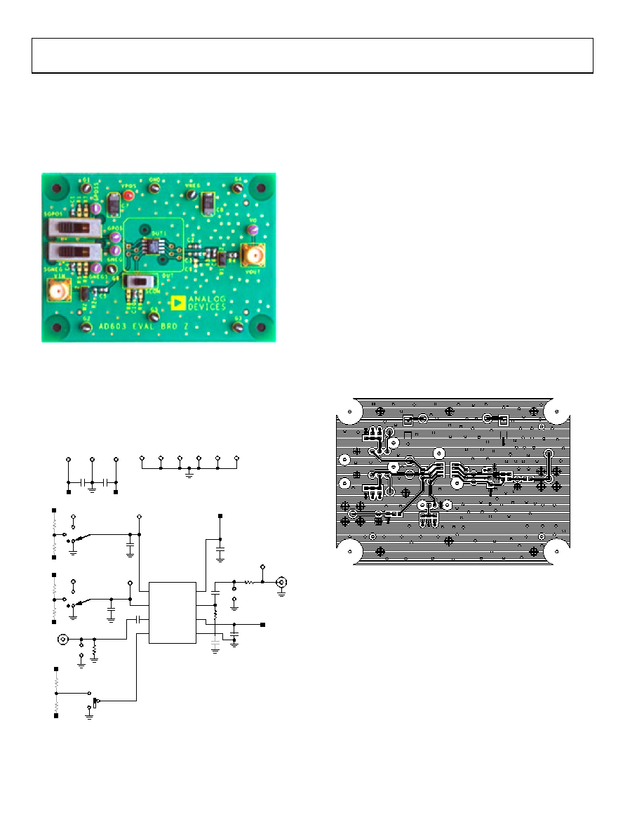
EVALUATION BOARD
The evaluation board of the AD603 enables simple bench-top
experimenting to be performed with easy control of the
AD603. Built-in flexibility allows convenient configuration to
accommodate most operating configurations. Figure 50 is a
photograph of the AD603 evaluation board.
00539-
049
Figure 50. AD603 Evaluation Board
Any dual-polarity power supply capable of providing 20 mA is
all that is required, in addition to whatever test equipment the
user wishes to perform the intended tests.
Referring to the schematic in Figure 51, the input to the VGA is
single-ended, ac-coupled, and terminated in 50 to accommodate
most commonly available signal generators.
SCOM
G1
G2
G3
G4
G5
G6
+
GPOS
VINP
VNEG
VOUT
VPOS
GNEG
COMM FDBK
VNEG
VPOS
GND
VNEG
VPOS
R7
R1
GPOS
GPOSS
SGPOS
SGNEG
GNEG
VPOS
VNEG
R6
R5
GNEGS
VPOS
VIN
R8
R9
C2
0.1F
C6
0.1F
C3
0.1F
R3
0
C1
0.1F
C4
0.1F
C5
0.1F
W2
4
3
2
1
5
6
7
8
R2
100
AD603
R4
453
W1
VO
VOUT
VNEG
C9
C7
10F
25V
C8
10F
25V
00539-
050
Figure 51. Schematic of the AD603 Evaluation Board
The output is also ac-coupled and includes a 453 series resistor.
Set the AD603 gain by connecting a voltage source between the
GNEG and GPOS test loops. The two slide switches SGPOS and
SGNEG provide three connections for GPOS and the GNEG.
Either pin can be ground referenced, or biased with a user selected
voltage established by R1 and R5 to R7. A signal generator can
be connected to the GPOS or GNEG test loops, or the GNEG can
be driven to either polarity within the common-mode limits of
1.2 V to +2.0 V; to invert the gain slope, simply reverse the
polarity of the voltage source connected to GPOS and GNEG.
For bias current measurements, the third switch option
disconnects the bias voltage source and permits connection of a
microammeter between the GPOS and GNEG pins to ground.
The AD603 includes built-in gain resistors selectable at the
FDBK pin. The board is shipped with the gain at minimum,
with a 0 resistor installed in R3. For maximum gain, simply
remove R3. Because of the architecture of the AD603, the
bandwidth decreases by 10, but the gain range remains at 40 dB.
Intermediate gain values may be selected by installing a resistor
between the VOUT and FDBK pins.
circuit side copper patterns and silkscreen.
00539-
051
Figure 52. Component Side Copper
相关PDF资料 |
PDF描述 |
|---|---|
| AD5750BCPZ | IC CURR/VOLT OUT DVR 32LFCSP |
| SM6S20AHE3/2D | TVS 6W 20V 5% SMD DO-218AB |
| SM6S18AHE3/2D | TVS 6W 18V 5% SMD DO-218AB |
| SM6S17AHE3/2D | TVS 6W 17V 5% SMD DO-218AB |
| SM6S16AHE3/2D | TVS 6W 16V 5% SMD DO-218AB |
相关代理商/技术参数 |
参数描述 |
|---|---|
| AD603ARZ-REEL7 | 功能描述:IC AMP VGA 90MHZ LN 50MA 8SOIC RoHS:是 类别:集成电路 (IC) >> Linear - Amplifiers - Instrumentation 系列:X-AMP® 标准包装:150 系列:- 放大器类型:音频 电路数:2 输出类型:- 转换速率:5 V/µs 增益带宽积:12MHz -3db带宽:- 电流 - 输入偏压:100nA 电压 - 输入偏移:500µV 电流 - 电源:6mA 电流 - 输出 / 通道:50mA 电压 - 电源,单路/双路(±):4 V ~ 32 V,±2 V ~ 16 V 工作温度:-40°C ~ 85°C 安装类型:表面贴装 封装/外壳:8-TSSOP(0.173",4.40mm 宽) 供应商设备封装:8-TSSOP 包装:管件 |
| AD603-EB | 制造商:Analog Devices 功能描述:Evaluation Board For Low Noise, 90 MHz Variable Gain Amplifier |
| AD603-EVALZ | 功能描述:BOARD EVALUATION FOR AD603 RoHS:是 类别:编程器,开发系统 >> 评估板 - 运算放大器 系列:X-AMP® 产品培训模块:Lead (SnPb) Finish for COTS Obsolescence Mitigation Program 标准包装:1 系列:- |
| AD603SQ/883B | 功能描述:差分放大器 IC 90 MHz VARIABLE GAIN AMP RoHS:否 制造商:Analog Devices 通道数量:1 Channel 带宽:900 MHz 可用增益调整:5.6 dB to 20 dB 输入补偿电压:1 mV at 5 V 共模抑制比(最小值):67 dB 工作电源电压:11 V 电源电流:28 mA 最大工作温度:+ 85 C 最小工作温度:- 40 C 安装风格:SMD/SMT 封装 / 箱体:SOIC-8 封装:Reel |
| AD603SQ/883B2 | 制造商:AD 制造商全称:Analog Devices 功能描述:Low Noise, 90 MHz Variable Gain Amplifier |
发布紧急采购,3分钟左右您将得到回复。