参数资料
| 型号: | AD640JNZ |
| 厂商: | Analog Devices Inc |
| 文件页数: | 2/16页 |
| 文件大小: | 0K |
| 描述: | IC AMP LOG 2.3MA 20DIP |
| 标准包装: | 1 |
| 放大器类型: | 对数 |
| 电路数: | 1 |
| -3db带宽: | 350MHz |
| 电流 - 输入偏压: | 7µA |
| 电压 - 输入偏移: | 50µV |
| 电流 - 电源: | 35mA |
| 电流 - 输出 / 通道: | 2.3mA |
| 电压 - 电源,单路/双路(±): | ±4.5 V ~ 7.5 V |
| 工作温度: | 0°C ~ 70°C |
| 安装类型: | 通孔 |
| 封装/外壳: | 20-DIP(0.300",7.62mm) |
| 供应商设备封装: | 20-PDIP |
| 包装: | 管件 |
AD640
REV. C
–10–
Table I.
Input
Peak
Intercept
Error (Relative
Waveform
or RMS
Factor
to a DC Input)
Square Wave
Either
1
0.00 dB
Sine Wave
Peak
2
–6.02 dB
Sine Wave
rms
1.414(
√2)
–3.01 dB
Triwave
Peak
2.718 (e)
–8.68 dB
Triwave
rms
1.569(e/
√3)
–3.91 dB
Gaussian Noise
rms
1.887
–5.52 dB
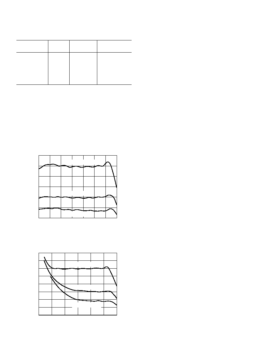
Logarithmic Conformance and Waveform
The waveform also affects the ripple, or periodic deviation from
an ideal logarithmic response. The ripple is greatest for dc or
square wave inputs because every value of the input voltage
maps to a single location on the transfer function and thus
traces out the full nonlinearities in the logarithmic response.
By contrast, a general time varying signal has a continuum of
values within each cycle of its waveform. The averaged output is
thereby “smoothed” because the periodic deviations away from
the ideal response, as the waveform “sweeps over” the transfer
function, tend to cancel. This smoothing effect is greatest for a
triwave input, as demonstrated in Figure 22.
INPUT AMPLITUDE IN dB ABOVE 1V, AT 10kHz
2
–10
–80
DEVIATION
FROM
EXACT
LOGARITHMIC
TRANSFER
FUNCTION
–
dB
–8
–6
–4
–2
0
–70
–60
–50
–40
–30
–20
–10
SQUARE WAVE INPUT
SINE WAVE INPUT
TRIWAVE INPUT
Figure 22. Deviation from Exact Logarithmic Transfer
Function for Two Cascaded AD640s, Showing Effect of
Waveform on Calibration and Linearity
INPUT AMPLITUDE IN dB ABOVE 1V, AT 10kHz
2
–10
DEVIATION
FROM
EXACT
LOGARITHMIC
TRANSFER
FUNCTION
–
dB
–8
–6
–4
–2
0
–70
–60
–50
–40
–30
–20
–10
SQUARE WAVE INPUT
SINE WAVE INPUT
TRIWAVE INPUT
–12
4
Figure 23. Deviation from Exact Logarithmic Transfer
Function for a Single AD640; Compare Low Level
Response with that of Figure 22
The accuracy at low signal inputs is also waveform dependent.
The detectors are not perfect absolute value circuits, having a
sharp “corner” near zero; in fact they become parabolic at low
levels and behave as if there were a dead zone. Consequently,
the output tends to be higher than ideal. When there are enough
stages in the system, as when two AD640s are connected in
cascade, most detectors will be adequately loaded due to the
high overall gain, but a single AD640 does not have sufficient
gain to maintain high accuracy for low level sine wave or triwave
inputs. Figure 23 shows the absolute deviation from calibration
for the same three waveforms for a single AD640. For inputs
between –10 dBV and –40 dBV the vertical displacement of the
traces for the various waveforms remains in agreement with the
predicted dependence, but significant calibration errors arise at
low signal levels.
SIGNAL MAGNITUDE
AD640 is a calibrated device. It is, therefore, important to be
clear in specifying the signal magnitude under all waveform
conditions. For dc or square wave inputs there is, of course, no
ambiguity. Bounded periodic signals, such as sinusoids and
triwaves, can be specified in terms of their simple amplitude
(peak value) or alternatively by their rms value (which is a mea-
sure of power when the impedance is specified). It is generally bet-
ter to define this type of signal in terms of its amplitude because
the AD640 response is a consequence of the input voltage, not
power. However, provided that the appropriate value of inter-
cept for a specific waveform is observed, rms measures may be
used. Random waveforms can only be specified in terms of rms
value because their peak value may be unbounded, as is the case
for Gaussian noise. These must be treated on a case-by-case
basis. The effective intercept given in Table I should be used for
Gaussian noise inputs.
On the other hand, for bounded signals the amplitude can be
expressed either in volts or dBV (decibels relative to 1 V). For
example, a sine wave or triwave of 1 mV amplitude can also be
defined as an input of –60 dBV, one of 100 mV amplitude as
–20 dBV, and so on. RMS value is usually expressed in dBm
(decibels above 1 mW) for a specified impedance level. Through-
out this data sheet we assume a 50
environment, the customary
impedance level for high speed systems, when referring to signal power
in dBm. Bearing in mind the above discussion of the effect of
waveform on the intercept calibration of the AD640, it will be
apparent that a sine wave at a power of, say, –10 dBm will not
produce the same output as a triwave or square wave of the
same power. Thus, a sine wave at a power level of –10 dBm has
an rms value of 70.7 mV or an amplitude of 100 mV (that is,
√2
times as large, the ratio of amplitude to rms value for a sine
wave), while a triwave of the same power has an amplitude
which is
√3 or 1.73 times its rms value, or 122.5 mV.
“Intercept” and “Logarithmic Offset”
If the signals are expressed in dBV, we can write the output in a
simpler form, as
IOUT = 50
A (Input
dBV – XdBV)
Equation (4)
where InputdBV is the input voltage amplitude (not rms) in dBV
and XdBV is the appropriate value of the intercept (for a given
waveform) in dBV. This form shows more clearly why the intercept
is often referred to as the logarithmic offset. For dc or square
wave inputs, VX is 1 mV so the numerical value of XdBV is –60,
and Equation (4) becomes
相关PDF资料 |
PDF描述 |
|---|---|
| 2524-6003UB | CONN HEADER 24POS STR GOLD T/H |
| 2516-5003UB | CONN HEADER 16POS R/A GOLD T/H |
| 2524-5002UB | SHROUDED HEADER 24 POS RT ANGLE |
| TMM-108-02-L-D | CONN HEADER 16POS DBL 2MM T/H |
| 77317-812-34LF | CONN HEADER .100 2ROW R/A 34POS |
相关代理商/技术参数 |
参数描述 |
|---|---|
| AD640JNZ | 制造商:Analog Devices 功能描述:Operational Amplifier (Op-Amp) IC |
| AD640JP | 功能描述:IC AMP LOG 2.3MA 20PLCC RoHS:否 类别:集成电路 (IC) >> Linear - Amplifiers - Instrumentation 系列:- 其它有关文件:TS1854A View All Specifications 标准包装:50 系列:- 放大器类型:通用 电路数:4 输出类型:满摆幅 转换速率:0.25 V/µs 增益带宽积:630kHz -3db带宽:- 电流 - 输入偏压:16nA 电压 - 输入偏移:1000µV 电流 - 电源:162µA 电流 - 输出 / 通道:48mA 电压 - 电源,单路/双路(±):1.8 V ~ 6 V 工作温度:-40°C ~ 125°C 安装类型:表面贴装 封装/外壳:14-SOIC(0.154",3.90mm 宽) 供应商设备封装:14-SO 包装:管件 |
| AD640JP-REEL | 制造商:Rochester Electronics LLC 功能描述:- Tape and Reel |
| AD640JP-REEL7 | 功能描述:IC AMP LOG 2.3MA 20PLCC RoHS:否 类别:集成电路 (IC) >> Linear - Amplifiers - Instrumentation 系列:- 标准包装:2,500 系列:- 放大器类型:通用 电路数:1 输出类型:满摆幅 转换速率:0.11 V/µs 增益带宽积:350kHz -3db带宽:- 电流 - 输入偏压:4nA 电压 - 输入偏移:20µV 电流 - 电源:260µA 电流 - 输出 / 通道:20mA 电压 - 电源,单路/双路(±):2.7 V ~ 36 V,±1.35 V ~ 18 V 工作温度:-40°C ~ 85°C 安装类型:表面贴装 封装/外壳:8-SOIC(0.154",3.90mm 宽) 供应商设备封装:8-SO 包装:带卷 (TR) |
| AD640JPZ | 功能描述:IC AMP LOG 2.3MA 20PLCC RoHS:是 类别:集成电路 (IC) >> Linear - Amplifiers - Instrumentation 系列:- 其它有关文件:TS1854A View All Specifications 标准包装:50 系列:- 放大器类型:通用 电路数:4 输出类型:满摆幅 转换速率:0.25 V/µs 增益带宽积:630kHz -3db带宽:- 电流 - 输入偏压:16nA 电压 - 输入偏移:1000µV 电流 - 电源:162µA 电流 - 输出 / 通道:48mA 电压 - 电源,单路/双路(±):1.8 V ~ 6 V 工作温度:-40°C ~ 125°C 安装类型:表面贴装 封装/外壳:14-SOIC(0.154",3.90mm 宽) 供应商设备封装:14-SO 包装:管件 |
发布紧急采购,3分钟左右您将得到回复。