参数资料
| 型号: | AD640JNZ |
| 厂商: | Analog Devices Inc |
| 文件页数: | 7/16页 |
| 文件大小: | 0K |
| 描述: | IC AMP LOG 2.3MA 20DIP |
| 标准包装: | 1 |
| 放大器类型: | 对数 |
| 电路数: | 1 |
| -3db带宽: | 350MHz |
| 电流 - 输入偏压: | 7µA |
| 电压 - 输入偏移: | 50µV |
| 电流 - 电源: | 35mA |
| 电流 - 输出 / 通道: | 2.3mA |
| 电压 - 电源,单路/双路(±): | ±4.5 V ~ 7.5 V |
| 工作温度: | 0°C ~ 70°C |
| 安装类型: | 通孔 |
| 封装/外壳: | 20-DIP(0.300",7.62mm) |
| 供应商设备封装: | 20-PDIP |
| 包装: | 管件 |
AD640
REV. C
–15–
diminishes the risk of instability due to poor grounding. Never-
theless, it must be remembered that at high frequencies even
very small lengths of wire, including the leads to capacitors,
have significant impedance. The ground plane itself can also
generate small but troublesome voltages due to circulating cur-
rents in a poor layout. A printed circuit evaluation board is
available from Analog Devices (Part Number ADEB640) to
facilitate the prototyping of an application using one or two
AD640s, plus various external components.
At very low signal levels various effects can cause significant
deviation from the ideal response, apart from the inherent non-
linearities of the transfer function already discussed. Note that
any spurious signal presented to the AD640s is demodulated and
added to the output. Thus, in the absence of thorough shielding,
emissions from any radio transmitters or RFI from equipment
operating in the locality will cause the output to appear too
high. The only cure for this type of error is the use of very care-
ful grounding and shielding techniques.
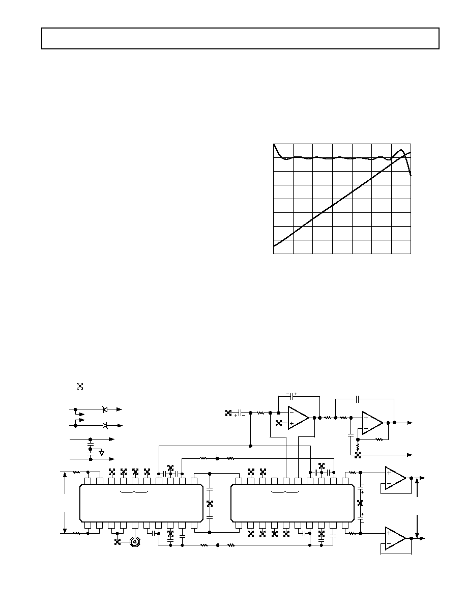
50 MHz–150 MHz Converter with 70 dB Dynamic Range
Figure 30 shows a logarithmic converter using two AD640s
which can provide at least 70 dB of dynamic range, limited
mostly by first stage noise. In this application, an rf choke (L1)
prevents the transmission of dc offset from the first to the sec-
ond AD640. One or two turns in a ferrite core will generally
suffice for operation at frequencies above 30 MHz. For ex-
ample, one complete loop of 20 gauge wire through the two
holes in a Fair-Rite type 2873002302 core provides an inductance
of 5
H, which presents an impedance of 1.57 k at 50 MHz.
The shunting effect across the 150
differential impedance at
the signal interface is thus fairly slight.
The signal source is optionally terminated by R1. To minimize
the input offset voltage R2 should be chosen to match the dc
resistance of the terminated source. (However, the offset voltage
is not a critical consideration in this ac-coupled application.)
Note that all unused inputs are grounded; this improves the
isolation from the outputs back to the inputs.
A transimpedance op amp (U3, AD844) converts the summed
logarithmic output currents of U1 and U2 to a ground referenced
voltage scaled 1 V per decade. The resistor R5 is nominally 1 k
but is increased slightly to compensate for the slope deficit at the
operating frequency, which can be determined from Figure 12.
The inverting input of U3 forms a virtual ground, so that each
logarithmic output of U1 and U2 is loaded by 100
(R3 or
R4). These resistors in conjunction with capacitors C1 and C2
form independent low-pass filters with a time constant of about
INPUT LEVEL – dBm IN 50
0
–60
–50
–40
–30
–20
–10
0
+1
–1
ERROR
–
dB
4
1
0
–70
LOW-PASS
FILTERED
OUTPUT
–
V
2
3
Figure 31. Logarithmic Output and Nonlinearity for Circuit
of Figure 30, for a Sine Wave Input at f = 80 MHz
5 ns. These capacitors should be connected directly across Pins
13 and 14, as shown, to prevent high frequency output currents
from circulating in the ground plane. A second 5 ns time con-
stant is formed by feedback resistor R5 in conjunction with the
transcapacitance of U3.
This filtering is adequate for input frequencies of 50 MHz or
above; more elaborate filtering can be devised for pulse
applications requiring a faster rise time. In applications where
only a long term measure of the input is needed, C1 and C2 can
5k
0.1 F
+15V
–15V
TO U3
AND U4
15
13
14
16
19
18
17
11
12
20
6
8
7
5
3
4
9
1
2
10
SIG
+IN
ATN
OUT
CKT
COM
RG1 RG0 RG2 LOG
OUT
LOG
COM
+VS SIG
+OUT
SIG
–IN
ATN
LO
ATN
COM
BL1
BL2
ITC
–VS
SIG
–OUT
1k
ATN
COM
ATN
IN
U2 AD640
C6
0.1 F
68
+6V
68
R7
3.3M
1/2
AD712
DENOTES A CONNECTION TO THE GROUND PLANE;
OBSERVE COMMON CONNECTIONS WHERE SHOWN.
ALL UNMARKED CAPACITORS ARE 0.1 F CERAMIC.
OFFSET
NULLING
FEEDBACK
U4a
5k
SIGNAL INPUT
15
13
14
16
19
18
17
11
12
20
SIG
+IN
ATN
OUT
CKT
COM
RG1 RG0 RG2 LOG
OUT
LOG
COM
+VS SIG
+OUT
SIG
–IN
ATN
LO
ATN
COM
BL1
BL2
ITC
–VS
SIG
–OUT
1k
ATN
COM
ATN
IN
U1 AD640
6
8
7
5
3
49
12
10
C1
(SEE
TEXT)
C2
(SEE
TEXT)
C7
4.7 F
C8
4.7 F
1
2
3
B
OFFSET
NULLING
FEEDBACK
U4b
7
6
5
A
1/2
AD712
1/2
AD712
U3a
1
2
3
NC
R2
50k
R3
50k
U3b
1/2
AD712
7
6
5
R4
200k
R5
200k
LOG
OUTPUT
+100mV/dB
C4
4.7 F
R1
49.9
C3
100 F
C5
0.1 F
A
B
+15V
–15V
TO U1
AND U2
TO U3
AND U4
9.1V
+6V
–6V
18
–6V
18
NC = NO CONNECT
R6
3.3M
Figure 32. Complete 95 dB Dynamic Range Converter
相关PDF资料 |
PDF描述 |
|---|---|
| 2524-6003UB | CONN HEADER 24POS STR GOLD T/H |
| 2516-5003UB | CONN HEADER 16POS R/A GOLD T/H |
| 2524-5002UB | SHROUDED HEADER 24 POS RT ANGLE |
| TMM-108-02-L-D | CONN HEADER 16POS DBL 2MM T/H |
| 77317-812-34LF | CONN HEADER .100 2ROW R/A 34POS |
相关代理商/技术参数 |
参数描述 |
|---|---|
| AD640JNZ | 制造商:Analog Devices 功能描述:Operational Amplifier (Op-Amp) IC |
| AD640JP | 功能描述:IC AMP LOG 2.3MA 20PLCC RoHS:否 类别:集成电路 (IC) >> Linear - Amplifiers - Instrumentation 系列:- 其它有关文件:TS1854A View All Specifications 标准包装:50 系列:- 放大器类型:通用 电路数:4 输出类型:满摆幅 转换速率:0.25 V/µs 增益带宽积:630kHz -3db带宽:- 电流 - 输入偏压:16nA 电压 - 输入偏移:1000µV 电流 - 电源:162µA 电流 - 输出 / 通道:48mA 电压 - 电源,单路/双路(±):1.8 V ~ 6 V 工作温度:-40°C ~ 125°C 安装类型:表面贴装 封装/外壳:14-SOIC(0.154",3.90mm 宽) 供应商设备封装:14-SO 包装:管件 |
| AD640JP-REEL | 制造商:Rochester Electronics LLC 功能描述:- Tape and Reel |
| AD640JP-REEL7 | 功能描述:IC AMP LOG 2.3MA 20PLCC RoHS:否 类别:集成电路 (IC) >> Linear - Amplifiers - Instrumentation 系列:- 标准包装:2,500 系列:- 放大器类型:通用 电路数:1 输出类型:满摆幅 转换速率:0.11 V/µs 增益带宽积:350kHz -3db带宽:- 电流 - 输入偏压:4nA 电压 - 输入偏移:20µV 电流 - 电源:260µA 电流 - 输出 / 通道:20mA 电压 - 电源,单路/双路(±):2.7 V ~ 36 V,±1.35 V ~ 18 V 工作温度:-40°C ~ 85°C 安装类型:表面贴装 封装/外壳:8-SOIC(0.154",3.90mm 宽) 供应商设备封装:8-SO 包装:带卷 (TR) |
| AD640JPZ | 功能描述:IC AMP LOG 2.3MA 20PLCC RoHS:是 类别:集成电路 (IC) >> Linear - Amplifiers - Instrumentation 系列:- 其它有关文件:TS1854A View All Specifications 标准包装:50 系列:- 放大器类型:通用 电路数:4 输出类型:满摆幅 转换速率:0.25 V/µs 增益带宽积:630kHz -3db带宽:- 电流 - 输入偏压:16nA 电压 - 输入偏移:1000µV 电流 - 电源:162µA 电流 - 输出 / 通道:48mA 电压 - 电源,单路/双路(±):1.8 V ~ 6 V 工作温度:-40°C ~ 125°C 安装类型:表面贴装 封装/外壳:14-SOIC(0.154",3.90mm 宽) 供应商设备封装:14-SO 包装:管件 |
发布紧急采购,3分钟左右您将得到回复。