参数资料
| 型号: | AD640JNZ |
| 厂商: | Analog Devices Inc |
| 文件页数: | 5/16页 |
| 文件大小: | 0K |
| 描述: | IC AMP LOG 2.3MA 20DIP |
| 标准包装: | 1 |
| 放大器类型: | 对数 |
| 电路数: | 1 |
| -3db带宽: | 350MHz |
| 电流 - 输入偏压: | 7µA |
| 电压 - 输入偏移: | 50µV |
| 电流 - 电源: | 35mA |
| 电流 - 输出 / 通道: | 2.3mA |
| 电压 - 电源,单路/双路(±): | ±4.5 V ~ 7.5 V |
| 工作温度: | 0°C ~ 70°C |
| 安装类型: | 通孔 |
| 封装/外壳: | 20-DIP(0.300",7.62mm) |
| 供应商设备封装: | 20-PDIP |
| 包装: | 管件 |
AD640
REV. C
–13–
It may occasionally be desirable to attenuate the signal even
further. For example, the source may have a full-scale value of
±10 V, and since the basic range of the AD640 extends only to
±200 mV dc, an attenuation factor of ×50 might be chosen.
This may be achieved either by using an independent external
attenuator or more simply by adding a resistor in series with
ATN IN (Pin 5). In the latter case the resistor must be trimmed
to calibrate the intercept, since the input resistance at Pin 5 is
not guaranteed. A fixed resistor of 1 k
in series with a 500
variable resistor calibrate to an intercept of 50 mV (or –26 dBV)
for dc or square wave inputs and provide a
±10 V input range.
The intercept stability will be degraded to about 0.003 dB/
°C.
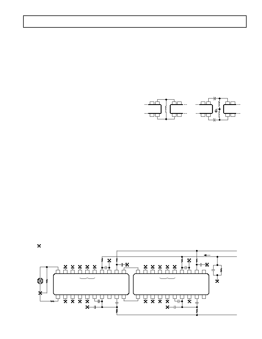
OPERATION OF CASCADED AD640S
Frequently, the dynamic range of the input will be 50 dB or
more. AD640s can be cascaded, as shown in Figure 27. The
balanced signal output from U1 becomes the input to U2. Re-
sistors are included in series with each LOG OUT pin and
capacitors C1 and C2 are placed directly between Pins 13 and 14
to provide a local path for the RF current at these output pairs.
C1 through C3 are chosen to provide the required low-pass
corner in conjunction with the load RL. Board layout and
grounding disciplines are critically important at the high gain
(X100,000) and bandwidth (~150 MHz) of this system.
The intercept voltage is calculated as follows. First, note that if
its LOG OUT is disconnected, U1 simply inserts 50 dB of
gain ahead of U2. This would lower the intercept by 50 dB, to
–110 dBV for square wave calibration. With the LOG OUT of
U1 added in, there is a finite zero signal current which slightly
shifts the intercept. With the intercept temperature compensa-
tion on U1 disabled this zero signal output is –270
A (see DC
SPECIFICATIONS) equivalent to a 5.4 dB upward shift in the
intercept, since the slope is 50
A/dB. Thus, the intercept is at
–104.6 dBV (–88.6 dBm for 50
sine calibration). ITC may be
disabled by grounding Pin 8 of either U1 or U2.
Cascaded AD640s can be used in dc applications, but input
offset voltage will limit the dynamic range. The dc intercept is
6
V. The offset should not be confused with the intercept, which is
found by extrapolating the transfer function from its central “log
linear” region. This can be understood by referring to Equation
(1) and noting that an input offset is simply additive to the value
of VIN in the numerator of the logarithmic argument; it does not
affect the denominator (or intercept) VX. In dc coupled applica-
tions of wide dynamic range, special precautions must be taken
to null the input offset and minimize drift due to input bias
offset. It is recommended that the input attenuator be used,
providing a practical input range of –74 dBV (
±200 V dc) to
+6 dBV (
±2 V dc) when nulled using the adjustment circuit
shown in Figure 25.
Eliminating the Effect of First Stage Offset
Usually, the input signal will be sinusoidal and U1 and U2 can
be ac coupled. Figure 28a shows a low resistance choke at the
input of U2 which shorts the dc output of U1 while preserving
the hf response. Coupling capacitors may be inserted (Fig-
ure 28b) in which case two chokes are used to provide bias
paths for U2. These chokes must exhibit high impedance over
the operating frequency range.
20
1
U2
U1
11
10
20
1
U2
U1
11
10
a.
b.
Figure 28. Two Methods for AC-Coupling AD640s
Alternatively, the input offset can be nulled by a negative feed-
back network from the SIG OUT nodes of U2 to the SIG IN
nodes of U1, as shown in Figure 29. The low-pass response of
the feedback path transforms to a closed-loop high-pass re-
sponse. The high gain (
×100,000) of the signal path results in a
commensurate reduction in the effective time constant of this
network. For example, to achieve a high-pass corner of 100 kHz,
the low-pass corner must be at 1 Hz.
In fact, it is somewhat more complicated than this. When the ac
input sufficiently exceeds that of the offset, the feedback be-
comes ineffective and the response becomes essentially dc
coupled. Even for quite modest inputs the last stage will be
limiting and the output (Pins 10 and 11) of U2 will be a square
wave of about
±180 mV amplitude, dwelling approximately
equal times at its two limit values, and thus having a net average
value near zero. Only when the input is very small does the high-
pass behavior of this nulling loop become apparent. Consequently,
the low-pass time constant can usually be reduced considerably
without serious performance degradation.
The resistor values are chosen such that the dc feedback is ade-
quate to null the worst case input offset, say, 500
V. There
RL= 50
C3
1mA/DECADE
15
13
14
16
19
18
17
11
12
20
6
8
7
5
3
4
10
9
1
2
SIG
+IN
ATN
OUT
CKT
COM
RG1 RG0 RG2 LOG
OUT
LOG
COM
+VS
SIG
+OUT
SIG
–IN
ATN
LO
ATN
COM
BL1
BL2
ITC
–VS
SIG
–OUT
1k
ATN
COM
ATN
IN
U1 AD640
NC
4.7
+5V
–5V
R1
R2
NC
15
13
14
16
19
18
17
11
12
20
6
8
7
5
3
4
10
9
1
2
SIG
+IN
ATN
OUT
CKT
COM
RG1 RG0 RG2 LOG
OUT
LOG
COM
+VS
SIG
+OUT
SIG
–IN
ATN
LO
ATN
COM
BL1
BL2
ITC
–VS
SIG
–OUT
1k
ATN
COM
ATN
IN
U2 AD640
C1
10
C2
10
OUTPUT
–50mV/DECADE
4.7
DENOTES A CONNECTION TO THE GROUND PLANE;
OBSERVE COMMON CONNECTIONS WHERE SHOWN.
ALL UNMARKED CAPACITORS ARE 0.1 F CERAMIC.
SEE TEXT FOR VALUES OF NUMBERED COMPONENTS.
SIGNAL
INPUT
NC = NO CONNECT
Figure 27. Basic Connections for Cascaded AD640s
相关PDF资料 |
PDF描述 |
|---|---|
| 2524-6003UB | CONN HEADER 24POS STR GOLD T/H |
| 2516-5003UB | CONN HEADER 16POS R/A GOLD T/H |
| 2524-5002UB | SHROUDED HEADER 24 POS RT ANGLE |
| TMM-108-02-L-D | CONN HEADER 16POS DBL 2MM T/H |
| 77317-812-34LF | CONN HEADER .100 2ROW R/A 34POS |
相关代理商/技术参数 |
参数描述 |
|---|---|
| AD640JNZ | 制造商:Analog Devices 功能描述:Operational Amplifier (Op-Amp) IC |
| AD640JP | 功能描述:IC AMP LOG 2.3MA 20PLCC RoHS:否 类别:集成电路 (IC) >> Linear - Amplifiers - Instrumentation 系列:- 其它有关文件:TS1854A View All Specifications 标准包装:50 系列:- 放大器类型:通用 电路数:4 输出类型:满摆幅 转换速率:0.25 V/µs 增益带宽积:630kHz -3db带宽:- 电流 - 输入偏压:16nA 电压 - 输入偏移:1000µV 电流 - 电源:162µA 电流 - 输出 / 通道:48mA 电压 - 电源,单路/双路(±):1.8 V ~ 6 V 工作温度:-40°C ~ 125°C 安装类型:表面贴装 封装/外壳:14-SOIC(0.154",3.90mm 宽) 供应商设备封装:14-SO 包装:管件 |
| AD640JP-REEL | 制造商:Rochester Electronics LLC 功能描述:- Tape and Reel |
| AD640JP-REEL7 | 功能描述:IC AMP LOG 2.3MA 20PLCC RoHS:否 类别:集成电路 (IC) >> Linear - Amplifiers - Instrumentation 系列:- 标准包装:2,500 系列:- 放大器类型:通用 电路数:1 输出类型:满摆幅 转换速率:0.11 V/µs 增益带宽积:350kHz -3db带宽:- 电流 - 输入偏压:4nA 电压 - 输入偏移:20µV 电流 - 电源:260µA 电流 - 输出 / 通道:20mA 电压 - 电源,单路/双路(±):2.7 V ~ 36 V,±1.35 V ~ 18 V 工作温度:-40°C ~ 85°C 安装类型:表面贴装 封装/外壳:8-SOIC(0.154",3.90mm 宽) 供应商设备封装:8-SO 包装:带卷 (TR) |
| AD640JPZ | 功能描述:IC AMP LOG 2.3MA 20PLCC RoHS:是 类别:集成电路 (IC) >> Linear - Amplifiers - Instrumentation 系列:- 其它有关文件:TS1854A View All Specifications 标准包装:50 系列:- 放大器类型:通用 电路数:4 输出类型:满摆幅 转换速率:0.25 V/µs 增益带宽积:630kHz -3db带宽:- 电流 - 输入偏压:16nA 电压 - 输入偏移:1000µV 电流 - 电源:162µA 电流 - 输出 / 通道:48mA 电压 - 电源,单路/双路(±):1.8 V ~ 6 V 工作温度:-40°C ~ 125°C 安装类型:表面贴装 封装/外壳:14-SOIC(0.154",3.90mm 宽) 供应商设备封装:14-SO 包装:管件 |
发布紧急采购,3分钟左右您将得到回复。