- 您现在的位置:买卖IC网 > PDF目录22164 > AD650KNZ (Analog Devices Inc)IC CONVERTER V-F/F-V 14DIP PDF资料下载
参数资料
| 型号: | AD650KNZ |
| 厂商: | Analog Devices Inc |
| 文件页数: | 10/20页 |
| 文件大小: | 385K |
| 描述: | IC CONVERTER V-F/F-V 14DIP |
| 标准包装: | 25 |
| 类型: | 电压至频率和频率至电压 |
| 频率 - 最大: | 1MHz |
| 全量程: | ±150ppm/°C |
| 线性: | ±0.1% |
| 安装类型: | 通孔 |
| 封装/外壳: | 14-DIP(0.300",7.62mm) |
| 供应商设备封装: | 14-PDIP |
| 包装: | 管件 |
| 产品目录页面: | 786 (CN2011-ZH PDF) |
AD650
Data Sheet
Rev. E | Page 10 of 20
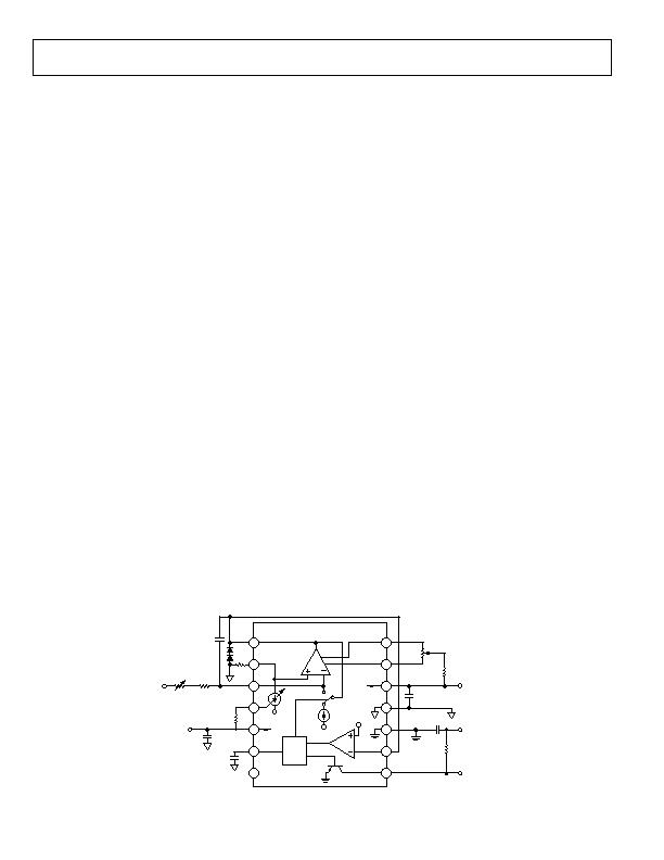
BIPOLAR V/F
Figure 11 shows how the internal bipolar current sink is used to
provide a half-scale offset for a ? V signal range, while providing
a 100 kHz maximum output frequency. The nominally 0.5 mA
(?0%) offset current sink is enabled when a 1.24 k?resistor is
connected between Pin 4 and Pin 5. Thus, with the grounded
10 k?nominal resistance shown, a 5 V offset is developed at
Pin 2. Because Pin 3 must also be at 5 V, the current through R
IN
is 10 V/40 k?= +0.25 mA at V
IN
= +5 V, and 0 mA at V
IN
= 5 V.
Components are selected using the same guidelines outlined for
the unipolar configuration with one alteration. The voltage
across the total signal range must be equated to the maximum
input voltage in the unipolar configuration. In other words, the
value of the input resistor RIN is determined by the input voltage
span, not the maximum input voltage. A diode from Pin 1 to
ground is also recommended. This is further discussed in the
Other Circuit Considerations section.
As in the unipolar circuit, R
IN
and C
OS
must have low temperature
coefficients to minimize the overall gain drift. The 1.24 k?
resistor used to activate the 0.5 mA offset current should also
have a low temperature coefficient. The bipolar offset current
has a temperature coefficient of approximately 200 ppm/癈.
UNIPOLAR V/F, NEGATIVE INPUT VOLTAGE
Figure 12 shows the connection diagram for V/F conversion of
negative input voltages. In this configuration, full-scale output
frequency occurs at negative full-scale input, and zero output
frequency corresponds with zero input voltage.
A very high impedance signal source can be used because it only
drives the noninverting integrator input. Typical input impedance
at this terminal is 1 G?or higher. For V/F conversion of positive
input signals using the connection diagram of Figure 4, the
signal generator must be able to source the integration current
to drive the AD650. For the negative V/F conversion circuit of
Figure 12, the integration current is drawn from ground
through R1 and R3, and the active input is high impedance.
Circuit operation for negative input voltages is very similar to
positive input unipolar conversion described in the Unipolar
Configuration section. For best operating results use Equation 7
and Equation 8 in the Component Selection section.
F/V CONVERSION
The AD650 also makes a very linear frequency-to-voltage
converter. Figure 13 shows the connection diagram for F/V
conversion with TTL input logic levels. Each time the input
signal crosses the comparator threshold going negative, the one
shot is activated and switches 1 mA into the integrator input for
a measured time period (determined by C
OS
). As the frequency
increases, the amount of charge injected into the integration
capacitor increases proportionately. The voltage across the
integration capacitor is stabilized when the leakage current
through R1 and R3 equals the average current being switched
into the integrator. The net result of these two effects is an
average output voltage that is proportional to the input
frequency. Optimum performance can be obtained by selecting
components using the same guidelines and equations listed in
the Bipolar V/F section.
For a more complete description of this application, refer to
Analog Devices Application Note AN-279.
HIGH FREQUENCY OPERATION
Proper RF techniques must be observed when operating the
AD650 at or near its maximum frequency of 1 MHz. Lead
lengths must be kept as short as possible, especially on the one
shot and integration capacitors, and at the integrator summing
junction. In addition, at maximum output frequencies above
500 kHz, a 3.6 k?pull-down resistor from Pin 1 to V
S
is
required (see Figure 14). The additional current drawn through
the pulldown resistor reduces the op amps output impedance
and improves its transient response.
OP
AMP
COMP
IN
FREQ
OUT
OUT
ONE
SHOT
8
9
10
11
13
12
7
6
5
4
3
2
1
14
INPUT
OFFSET
TRIM
0.6V
AD650
V
S
V
S
1mA
S1
C
OS
330pF
15V
0.1礔
V
IN
?V
1.24k&
R3
37.4k&
10k&
R1
5k&
C
INT
1000pF
20k&
250k&
0.1礔
1礔
1k&
+15V
+5V
DIGITAL
GND
ANALOG
GND
F
OUT
Figure 11. Connections for ? V Bipolar V/F with 0 kHz to 100 kHz TTL Output
相关PDF资料 |
PDF描述 |
|---|---|
| RBC13DRYN | CONN EDGECARD 26POS .100 EXTEND |
| IDT71256SA15TPI | IC SRAM 256KBIT 15NS 28DIP |
| VI-J1R-CX-F1 | CONVERTER MOD DC/DC 7.5V 75W |
| V28A36C200BG2 | CONVERTER MOD DC/DC 36V 200W |
| AD7741YRZ | IC CONVERTER VOLT TO FREQ 8SOIC |
相关代理商/技术参数 |
参数描述 |
|---|---|
| AD650KNZ | 制造商:Analog Devices 功能描述:IC VOLTAGE CONVERTER |
| AD650KP | 制造商:未知厂家 制造商全称:未知厂家 功能描述:Converter |
| AD650S | 制造商:AD 制造商全称:Analog Devices 功能描述:Voltage-to-Frequency and Frequency-to-Voltage Converter |
| AD650SD | 功能描述:IC V-F/F-V CONV 1MHZ 14-CDIP RoHS:否 类别:集成电路 (IC) >> PMIC - V/F 和 F/V 转换器 系列:- 标准包装:1 系列:- 类型:频率至电压 频率 - 最大:10kHz 全量程:- 线性:±0.3% 安装类型:表面贴装 封装/外壳:8-SOIC(0.154",3.90mm 宽) 供应商设备封装:8-SOIC 包装:Digi-Reel® 其它名称:LM2917MX-8/NOPBDKR |
| AD650SD/883B | 功能描述:电压频率转换及频率电压转换 IC - V/F CONVERTER IC RoHS:否 制造商:Texas Instruments 全标度频率:4000 KHz 线性误差:+/- 1 % FSR 电源电压-最大: 电源电压-最小: 最大工作温度:+ 85 C 最小工作温度:- 25 C 安装风格:Through Hole 封装 / 箱体:PDIP-14 封装:Tube |
发布紧急采购,3分钟左右您将得到回复。