- 您现在的位置:买卖IC网 > PDF目录22164 > AD650KNZ (Analog Devices Inc)IC CONVERTER V-F/F-V 14DIP PDF资料下载
参数资料
| 型号: | AD650KNZ |
| 厂商: | Analog Devices Inc |
| 文件页数: | 13/20页 |
| 文件大小: | 385K |
| 描述: | IC CONVERTER V-F/F-V 14DIP |
| 标准包装: | 25 |
| 类型: | 电压至频率和频率至电压 |
| 频率 - 最大: | 1MHz |
| 全量程: | ±150ppm/°C |
| 线性: | ±0.1% |
| 安装类型: | 通孔 |
| 封装/外壳: | 14-DIP(0.300",7.62mm) |
| 供应商设备封装: | 14-PDIP |
| 包装: | 管件 |
| 产品目录页面: | 786 (CN2011-ZH PDF) |
Data Sheet
AD650
Rev. E | Page 13 of 20
Other circuit components do not directly influence the accuracy
of the VFC over temperature changes as long as their actual
values are not as different from the nominal value as to preclude
operation. This includes the integration capacitor C
INT
. A change
in the capacitance value of C
INT
simply results in a different rate of
voltage change across the capacitor. During the integration phase
(see Figure 8), the rate of voltage change across C
INT
has the
opposite effect that it does during the reset phase. The result is
that the conversion accuracy is unchanged by either drift or
tolerance of CINT. The net effect of a change in the integrator
capacitor is simply to change the peak-to-peak amplitude of the
sawtooth waveform at the output of the integrator.
The gain temperature coefficient of the AD650 is not a constant
value. Rather, the gain TC is a function of both the full-scale
frequency and the ambient temperature. At a low full-scale
frequency, the gain TC is determined primarily by the stability of
the internal reference (a buried Zener reference). This low speed
gain TC can be quite effective; at 10 kHz full scale, the gain TC near
25癈 is typically 0 ?50 ppm/癈. Although the gain TC changes
with ambient temperature (tending to be more positive at higher
temperatures), the drift remains within a ?5 ppm/癈 window over
the entire military temperature range. At full-scale frequencies
higher than 10 kHz, dynamic errors become much more important
than the static drift of the dc reference. At a full-scale frequency
of 100 kHz and above, these timing errors dominate the gain
TC. For example, at 100 kHz full-scale frequency (RIN = 40 k?and
C
OS
= 330 pF) the gain TC near room temperature is typically
80 ?0 ppm/癈, but at an ambient temperature near 125癈, the
gain TC tends to be more positive and is typically 15 ?0 ppm/癈.
This information is presented in a graphical form in Figure 15.
The gain TC always tends to become more positive at higher
temperatures. Therefore, it is possible to adjust the gain TC of
the AD650 by using a one-shot capacitor with an appropriate
TC to cancel the drift of the circuit. For example, consider the
100 kHz full-scale frequency. An average drift of 100 ppm/癈
means that as temperature is increased, the circuit produces a
lower frequency in response to a given input voltage. This means
that the one-shot capacitor must decrease in value as temperature
increases in order to compensate the gain TC of the AD650; that
is, the capacitor must have a TC of 100 ppm/癈. Now consider
the 1 MHz full-scale frequency.
100
50
10kHz
100kHz
1MHz
25 0 25 50 75
100 125
0
100
200
300
400
TEMPERATURE (癈)
Figure 15. Gain TC vs. Temperature
It is not possible to achieve much improvement in performance
unless the expected ambient temperature range is known. For
example, in a constant low temperature application such as
gathering data in an Arctic climate (approximately 20癈), a
C
OS
with a drift of 310 ppm/癈 is called for in order to compensate
the gain drift of the AD650. However, if that circuit should see
an ambient temperature of 75癈, then the C
OS
capacitor would
change the gain TC from approximately 0 ppm to 310 ppm/癈.
The temperature effects of these components are the same when
the AD650 is configured for negative or bipolar input voltages,
and for F/V conversion as well.
NONLINEARITY SPECIFICATION
The linearity error of the AD650 is specified by the endpoint
method. That is, the error is expressed in terms of the deviation
from the ideal voltage to frequency transfer relation after
calibrating the converter at full scale and zero. The nonlinearity
varies with the choice of one-shot capacitor and input resistor
(see Figure 10). Verification of the linearity specification
requires the availability of a switchable voltage source (or a
DAC) having a linearity error below 20 ppm, and the use of
very long measurement intervals to minimize count
uncertainties. Every AD650 is automatically tested for linearity,
and it is not usually necessary to perform this verification,
which is both tedious and time consuming. If it is required to
perform a nonlinearity test either as part of an incoming quality
screening or as a final product evaluation, an automated bench-
top tester proves useful. Such a system based on Analog
Devices LTS-2010 is described in
V-F Converters Demand
Accurate Linearity Testing,
by L. DeVito, (Electronic Design,
March 4, 1982).
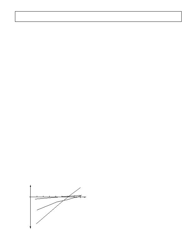
The voltage-to-frequency transfer relation is shown in Figure 16
and Figure 17 with the nonlinearity exaggerated for clarity. The
first step in determining nonlinearity is to connect the endpoints of
the operating range (typically at 10 mV and 10 V) with a straight
line. This straight line is then the ideal relationship that is desired
from the circuit. The second step is to find the difference between
this line and the actual response of the circuit at a few points
between the endpointstypically ten intermediate points
suffices. The difference between the actual and the ideal
response is a frequency error measured in hertz. Finally, these
frequency errors are normalized to the full-scale frequency and
expressed either as parts per million of full scale (ppm) or parts
per hundred of full scale (%). For example, on a 100 kHz full
scale, if the maximum frequency error is 5 Hz, the nonlinearity
is specified as 50 ppm or 0.005%. Typically on the 100 kHz
scale, the nonlinearity is positive and the maximum value
occurs at about midscale (Figure 16). At higher full-scale
frequencies, (500 kHz to 1 MHz), the nonlinearity becomes
S
shaped and the maximum value can be either positive or negative.
Typically, on the 1 MHz scale (RIN = 16.9 k? COS = 51 pF) the
nonlinearity is positive below about 2/3 scale and is negative
above this point. This is shown graphically in Figure 17.
相关PDF资料 |
PDF描述 |
|---|---|
| RBC13DRYN | CONN EDGECARD 26POS .100 EXTEND |
| IDT71256SA15TPI | IC SRAM 256KBIT 15NS 28DIP |
| VI-J1R-CX-F1 | CONVERTER MOD DC/DC 7.5V 75W |
| V28A36C200BG2 | CONVERTER MOD DC/DC 36V 200W |
| AD7741YRZ | IC CONVERTER VOLT TO FREQ 8SOIC |
相关代理商/技术参数 |
参数描述 |
|---|---|
| AD650KNZ | 制造商:Analog Devices 功能描述:IC VOLTAGE CONVERTER |
| AD650KP | 制造商:未知厂家 制造商全称:未知厂家 功能描述:Converter |
| AD650S | 制造商:AD 制造商全称:Analog Devices 功能描述:Voltage-to-Frequency and Frequency-to-Voltage Converter |
| AD650SD | 功能描述:IC V-F/F-V CONV 1MHZ 14-CDIP RoHS:否 类别:集成电路 (IC) >> PMIC - V/F 和 F/V 转换器 系列:- 标准包装:1 系列:- 类型:频率至电压 频率 - 最大:10kHz 全量程:- 线性:±0.3% 安装类型:表面贴装 封装/外壳:8-SOIC(0.154",3.90mm 宽) 供应商设备封装:8-SOIC 包装:Digi-Reel® 其它名称:LM2917MX-8/NOPBDKR |
| AD650SD/883B | 功能描述:电压频率转换及频率电压转换 IC - V/F CONVERTER IC RoHS:否 制造商:Texas Instruments 全标度频率:4000 KHz 线性误差:+/- 1 % FSR 电源电压-最大: 电源电压-最小: 最大工作温度:+ 85 C 最小工作温度:- 25 C 安装风格:Through Hole 封装 / 箱体:PDIP-14 封装:Tube |
发布紧急采购,3分钟左右您将得到回复。