- 您现在的位置:买卖IC网 > PDF目录22164 > AD650KNZ (Analog Devices Inc)IC CONVERTER V-F/F-V 14DIP PDF资料下载
参数资料
| 型号: | AD650KNZ |
| 厂商: | Analog Devices Inc |
| 文件页数: | 7/20页 |
| 文件大小: | 385K |
| 描述: | IC CONVERTER V-F/F-V 14DIP |
| 标准包装: | 25 |
| 类型: | 电压至频率和频率至电压 |
| 频率 - 最大: | 1MHz |
| 全量程: | ±150ppm/°C |
| 线性: | ±0.1% |
| 安装类型: | 通孔 |
| 封装/外壳: | 14-DIP(0.300",7.62mm) |
| 供应商设备封装: | 14-PDIP |
| 包装: | 管件 |
| 产品目录页面: | 786 (CN2011-ZH PDF) |
Data Sheet
AD650
Rev. E | Page 7 of 20
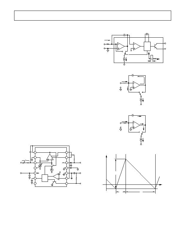
CIRCUIT OPERATION
UNIPOLAR CONFIGURATION
The AD650 is a charge balance voltage-to-frequency converter.
In the connection diagram shown in Figure 4, or the block
diagram of Figure 5, the input signal is converted into an
equivalent current by the input resistance R
IN
. This current is
exactly balanced by an internal feedback current delivered in
short, timed bursts from the switched 1 mA internal current
source. These bursts of current can be thought of as precisely
defined packets of charge. The required number of charge
packets, each producing one pulse of the output transistor,
depends upon the amplitude of the input signal. Because the
number of charge packets delivered per unit time is dependent
on the input signal amplitude, a linear voltage-to-frequency
transformation is accomplished. The frequency output is
furnished via an open collector transistor.
A more rigorous analysis demonstrates how the charge balance
voltage-to-frequency conversion takes place.
A block diagram of the device arranged as a V-to-F converter is
shown in Figure 5. The unit is comprised of an input integrator,
a current source and steering switch, a comparator, and a one
shot. When the output of the one shot is low, the current
steering switch S
1
diverts all the current to the output of the op
amp; this is called the integration period. When the one shot
has been triggered and its output is high, the switch S1 diverts
all the current to the summing junction of the op amp; this is
called the reset period. The two different states are shown in
Figure 6 and Figure 7 along with the various branch currents. It
should be noted that the output current from the op amp is the
same for either state, thus minimizing transients.
OP
AMP
COMP
IN
FREQ
OUT
OUT
ONE
SHOT
8
9
10
11
12
13
7
15V
0.1礔
C
OS
6
4
2
1
14
INPUT
OFFSET
TRIM
0.6V
AD650
V
S
V
S
1mA
S1
5
F
OUT
V
LOGIC
+15V
V
IN
R3 R1
R
IN
3
DIGITAL
GROUND
ANALOG
GROUND
1礔
250k&
20k&
R2
0.1礔
C
INT
Figure 4. Connection Diagram for V/F Conversion, Positive Input Voltage
V
IN
V
S
S1
1mA ?20%
AD650
+
R
IN
I
IN
C
INT
INTEGRATOR
0.6V
COMPARATOR
FREQUENCY
OUTPUT
ONE
SHOT
C
OS
t
t
OS
Figure 5. Block Diagram
V
IN
V
S
S1
1mA
R
IN
I
IN
C
INT
1mA I
IN
1mA
Figure 6. Reset Mode
V
IN
V
S
S1
1mA
R
IN
I
IN
C
INT
1mA I
IN
I
IN
1mA
Figure 7. Integrate Mode
RESET
INTEGRATE
0.6
V
t
OS
T
1
t
Figure 8. Voltage Across C
INT
相关PDF资料 |
PDF描述 |
|---|---|
| RBC13DRYN | CONN EDGECARD 26POS .100 EXTEND |
| IDT71256SA15TPI | IC SRAM 256KBIT 15NS 28DIP |
| VI-J1R-CX-F1 | CONVERTER MOD DC/DC 7.5V 75W |
| V28A36C200BG2 | CONVERTER MOD DC/DC 36V 200W |
| AD7741YRZ | IC CONVERTER VOLT TO FREQ 8SOIC |
相关代理商/技术参数 |
参数描述 |
|---|---|
| AD650KNZ | 制造商:Analog Devices 功能描述:IC VOLTAGE CONVERTER |
| AD650KP | 制造商:未知厂家 制造商全称:未知厂家 功能描述:Converter |
| AD650S | 制造商:AD 制造商全称:Analog Devices 功能描述:Voltage-to-Frequency and Frequency-to-Voltage Converter |
| AD650SD | 功能描述:IC V-F/F-V CONV 1MHZ 14-CDIP RoHS:否 类别:集成电路 (IC) >> PMIC - V/F 和 F/V 转换器 系列:- 标准包装:1 系列:- 类型:频率至电压 频率 - 最大:10kHz 全量程:- 线性:±0.3% 安装类型:表面贴装 封装/外壳:8-SOIC(0.154",3.90mm 宽) 供应商设备封装:8-SOIC 包装:Digi-Reel® 其它名称:LM2917MX-8/NOPBDKR |
| AD650SD/883B | 功能描述:电压频率转换及频率电压转换 IC - V/F CONVERTER IC RoHS:否 制造商:Texas Instruments 全标度频率:4000 KHz 线性误差:+/- 1 % FSR 电源电压-最大: 电源电压-最小: 最大工作温度:+ 85 C 最小工作温度:- 25 C 安装风格:Through Hole 封装 / 箱体:PDIP-14 封装:Tube |
发布紧急采购,3分钟左右您将得到回复。