- 您现在的位置:买卖IC网 > PDF目录22157 > AD652JP (Analog Devices Inc)IC V-F CONV SYNCH MONO 5V 20PLCC PDF资料下载
参数资料
| 型号: | AD652JP |
| 厂商: | Analog Devices Inc |
| 文件页数: | 22/28页 |
| 文件大小: | 779K |
| 描述: | IC V-F CONV SYNCH MONO 5V 20PLCC |
| 标准包装: | 1 |
| 类型: | 电压至频率 |
| 频率 - 最大: | 2MHz |
| 全量程: | ±25ppm/°C |
| 线性: | ±0.005% |
| 安装类型: | 表面贴装 |
| 封装/外壳: | 20-LCC(J 形引线) |
| 供应商设备封装: | 20-PLCC(9x9) |
| 包装: | 管件 |
第1页第2页第3页第4页第5页第6页第7页第8页第9页第10页第11页第12页第13页第14页第15页第16页第17页第18页第19页第20页第21页当前第22页第23页第24页第25页第26页第27页第28页
AD652
Rev. C | Page 22 of 28
ISOLATED FRONT END
In some applications, it may be necessary to have complete
galvanic isolation between the analog signals being measured
and the digital portions of the circuit. The circuit shown in
Figure 32 runs off a single 5 V power supply and provides a self-
contained, completely isolated analog measurement system. The
power for the AD652 SVFC is provided by a chopper and a
transformer, and is regulated to 15 V.
Both the chopper frequency and the AD652 clock frequency are
125 kHz, with the clock signal being relayed to the SVFC
through the transformer. The frequency output signal is relayed
through an opto-isolator and latched into a D flop. The chopper
frequency is generated from an AD654 VFC, and is frequency
divided by two to develop differential drive for the chopper
transistors, and to ensure an accurate 50% duty cycle. The pull-
up resistors on the D flop outputs provide a well-defined high
level voltage to the choppers to equalize the drive in each
direction. The 10 礖 inductor in the 5 V lead of the transformer
primary is necessary to equalize any residual imbalance in the
drive on each half cycle, and thus prevent saturation of the core.
The capacitor across the primary resonates the system so that
under light loading conditions on the secondary, the wave shape
is sinusoidal and the clock frequency is relayed to the SVFC. To
adjust the chopper frequency, disconnect any load on the
secondary and tune the AD654 for a minimum in the supply
current drawn from the 5 V supply.
A-TO-D CONVERSION
In performing an A-to-D conversion, the output pulses of a
VFC are counted for a fixed-gate interval. To achieve maximum
performance with the AD652, the fixed-gate interval should be
generated using a multiple of the SVFC clock input. Counting
in this manner eliminates any errors due to the clock (whether
it be jitter, drift with time or temperature, and so on) since it is
the ratio of the clock and output frequencies that is being
measured.
The resolution of the A-to-D conversion measurement is
determined by the clock frequency and the gate time. If, for
instance, a resolution of 12 bits is desired and the clock
frequency is 1 MHz (resulting in an AD652 FS frequency of
500 kHz) the gate time is:
( )
ms
192
.
8
sec
10
1
8192
4096
2
MHz
1
2
1
6
1
1
1
=
?/DIV>
=
?/DIV>
?/DIV>
?/DIV>
?/DIV>
?/DIV>
?/DIV>
?/DIV>
?/DIV>
=
?/DIV>
?/DIV>
?/DIV>
?/DIV>
?/DIV>
?/DIV>
?/DIV>
?/DIV>
=
?/DIV>
?/DIV>
?/DIV>
?/DIV>
?/DIV>
?/DIV>
?/DIV>
?/DIV>
N
Freq
Clock
N
Freq
FS
Where N is the total number of codes for a given resolution.
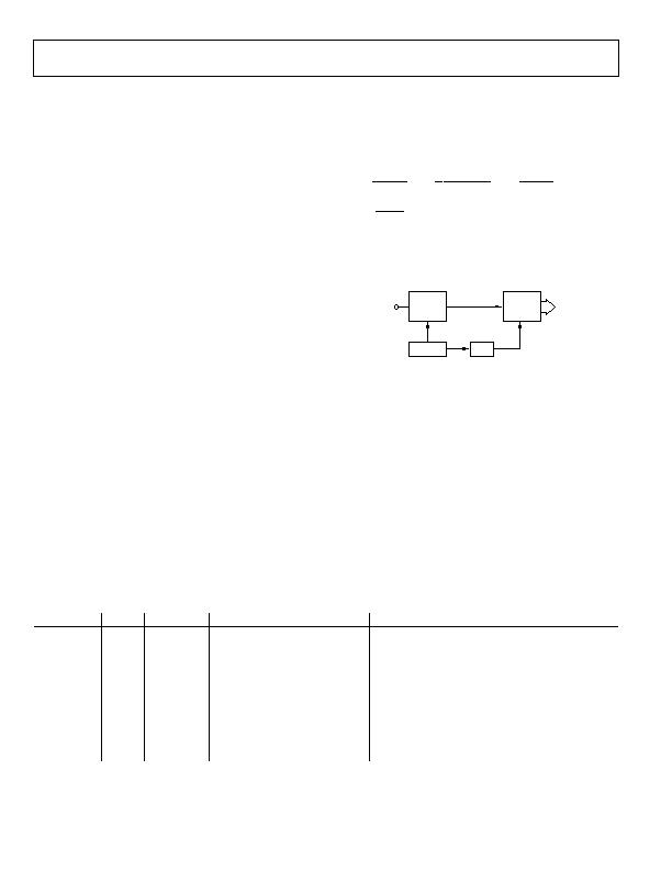
Figure 33 shows the AD652 SVFC as an A-to-D converter in
block diagram form.
IN
AD652
COUNTER TO?/SPAN>P
INPUT
GATE
f
OUT
CLOCK
?SPAN class="pst AD652SQ_2632819_9">2N
Figure 33. Block Diagram of SVFC A-to-D Converter
To provide the ?N block, a single-chip counter such as the
4020B can be used. The 4020B is a 14-stage binary ripple
counter that has a clock and master reset for inputs, and
buffered outputs from the first stage and the last 11 stages. The
output of the first stage is fCLOCK ?2
1
= fCLOCK/2, while the output
of the last stage is f
CLOCK
?2
14
= f
CLOCK
/16384. Therefore, using
this single chip counter as the ?N block, 13-bit resolution can
be achieved. Higher resolution can be achieved by cascading D-
type flip flops or another 4020B with the counter.
Table 4 shows the relationship between clock frequency and gate
time for various degrees of resolution. Note that if the variables
are chosen such that the gate times are multiples of 50 Hz,
60 Hz, or 400 Hz, normal mode rejection (NMR) of those line
frequencies occur.
Table 4.
Resolution N Clock
Conversion or Gate Time (ms) Typical Linearity (%) Comments
12 Bits
4096 81.92 kHz 100
0.002
50 Hz, 60 Hz,400 Hz NMR
12 Bits
4096 2 MHz
4.096
0.01
12 Bits
4096 4 MHz
2.048
0.02
4 Digits 10000 200 kHz 100
0.002
50 Hz, 60 Hz, 400 Hz NMR
14 Bits
16384 327.68 kHz 100
0.002
50 Hz, 60 Hz, 400 Hz NMR
14 Bits
16384 1.966 MHz 16.66
0.01
60 Hz NMR
14 Bits
16384 1.638 MHz 20
0.01
50 Hz NMR
4?Digits 20000 400 kHz 100
0.002
50 Hz, 60 Hz, 400 Hz NMR
16 Bits
65536 655.36 kHz 200
0.002
50 Hz, 60 Hz, 400 Hz NMR
16 Bits
65536 4 MHz
32.77
0.02
相关PDF资料 |
PDF描述 |
|---|---|
| GMC40DRAN | CONN EDGECARD 80POS R/A .100 SLD |
| AD650JPZ | IC V-F/F-V CONV 1MHZ 20-PLCC |
| GSC40DRAH | CONN EDGECARD 80POS R/A .100 SLD |
| AD650JP | IC V-F/F-V CONV 1MHZ 20-PLCC |
| TAJB476M006RNJ | CAP TANT 47UF 6.3V 20% 1210 |
相关代理商/技术参数 |
参数描述 |
|---|---|
| AD652JP-REEL | 功能描述:IC V-F CONV SYNCH MONO 5V 20PLCC RoHS:否 类别:集成电路 (IC) >> PMIC - V/F 和 F/V 转换器 系列:- 标准包装:1 系列:- 类型:频率至电压 频率 - 最大:10kHz 全量程:- 线性:±0.3% 安装类型:表面贴装 封装/外壳:8-SOIC(0.154",3.90mm 宽) 供应商设备封装:8-SOIC 包装:Digi-Reel® 其它名称:LM2917MX-8/NOPBDKR |
| AD652JP-REEL7 | 功能描述:IC V-F CONV SYNCH MONO 5V 20PLCC RoHS:否 类别:集成电路 (IC) >> PMIC - V/F 和 F/V 转换器 系列:- 标准包装:1 系列:- 类型:频率至电压 频率 - 最大:10kHz 全量程:- 线性:±0.3% 安装类型:表面贴装 封装/外壳:8-SOIC(0.154",3.90mm 宽) 供应商设备封装:8-SOIC 包装:Digi-Reel® 其它名称:LM2917MX-8/NOPBDKR |
| AD652JPZ | 功能描述:IC V-F CONV SYNCH MONO 5V 20PLCC RoHS:是 类别:集成电路 (IC) >> PMIC - V/F 和 F/V 转换器 系列:- 标准包装:1 系列:- 类型:频率至电压 频率 - 最大:10kHz 全量程:- 线性:±0.3% 安装类型:表面贴装 封装/外壳:8-SOIC(0.154",3.90mm 宽) 供应商设备封装:8-SOIC 包装:Digi-Reel® 其它名称:LM2917MX-8/NOPBDKR |
| AD652JPZ-REEL | 功能描述:IC CONV VOLT-FREQ SYNC 20PLCC RoHS:是 类别:集成电路 (IC) >> PMIC - V/F 和 F/V 转换器 系列:- 标准包装:1 系列:- 类型:频率至电压 频率 - 最大:10kHz 全量程:- 线性:±0.3% 安装类型:表面贴装 封装/外壳:8-SOIC(0.154",3.90mm 宽) 供应商设备封装:8-SOIC 包装:Digi-Reel® 其它名称:LM2917MX-8/NOPBDKR |
| AD652JPZ-REEL7 | 功能描述:IC CONV VOLT-FREQ SYNC 20PLCC RoHS:是 类别:集成电路 (IC) >> PMIC - V/F 和 F/V 转换器 系列:- 标准包装:1 系列:- 类型:频率至电压 频率 - 最大:10kHz 全量程:- 线性:±0.3% 安装类型:表面贴装 封装/外壳:8-SOIC(0.154",3.90mm 宽) 供应商设备封装:8-SOIC 包装:Digi-Reel® 其它名称:LM2917MX-8/NOPBDKR |
发布紧急采购,3分钟左右您将得到回复。